Stress assisted current driven switching for magnetic memory applications

a magnetic memory and current driving technology, applied in the field of magnetic memory systems, can solve the problems of high switching current and difficulty in switching at low current for magnetic memory applications, and achieve the effect of avoiding high switching current and reducing the number of applications

Inactive Publication Date: 2007-10-16
SAMSUNG SEMICON
View PDF13 Cites 181 Cited by
  • Summary
  • Abstract
  • Description
  • Claims
  • Application Information

AI Technical Summary

Benefits of technology

[0013]According to the system and method disclosed herein, the present invention provides a magnetic element that is capable of being written using a reduced current and that remains stable after being written.

Problems solved by technology

In particular, the magnetization may be difficult to switch at a low current, as will be described.
For a number of reasons, a high switching current is undesirable for magnetic memory application.

Method used


Image

  • Stress assisted current driven switching for magnetic memory applications
  • Stress assisted current driven switching for magnetic memory applications
  • Stress assisted current driven switching for magnetic memory applications

Examples


second embodiment

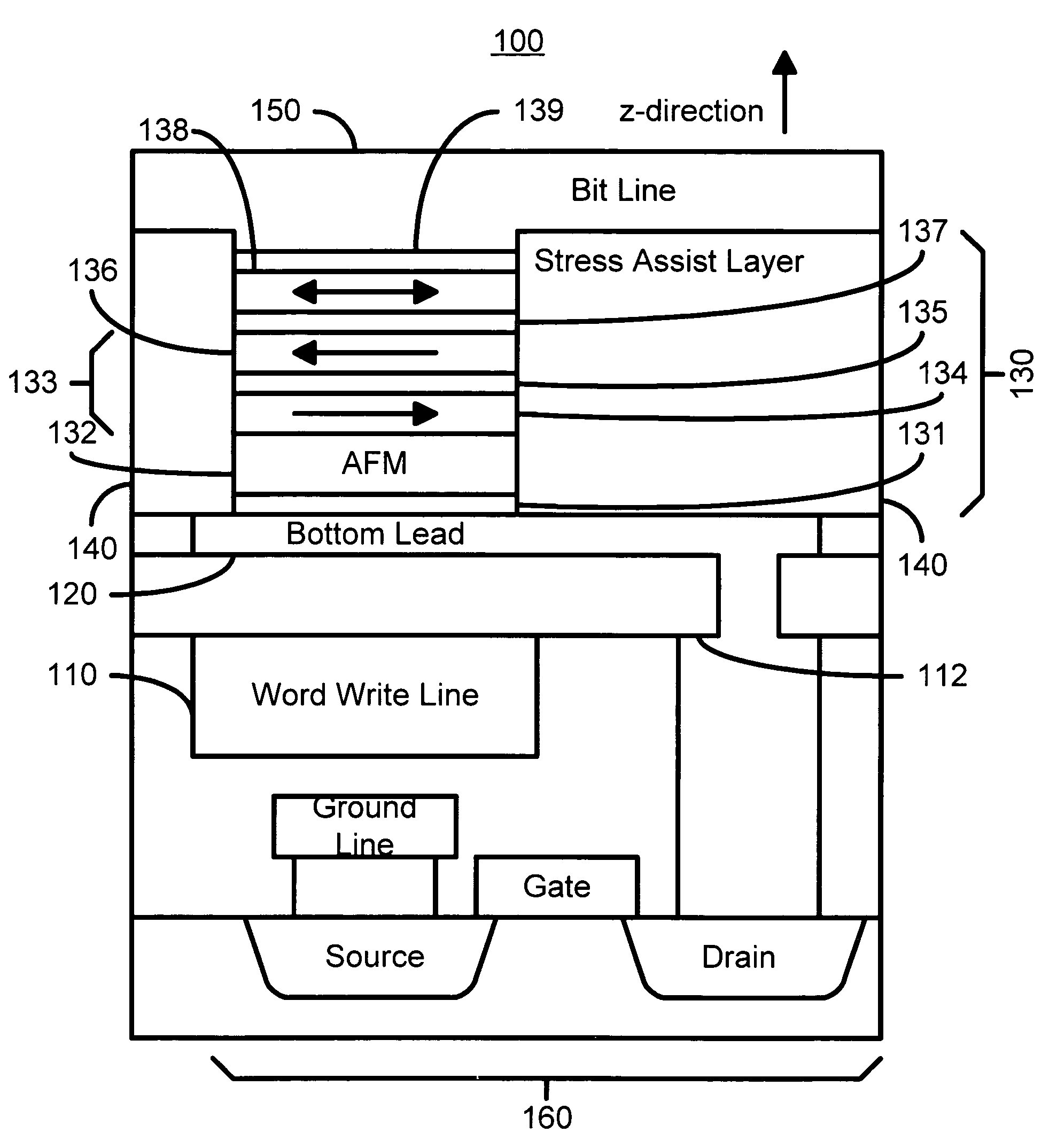
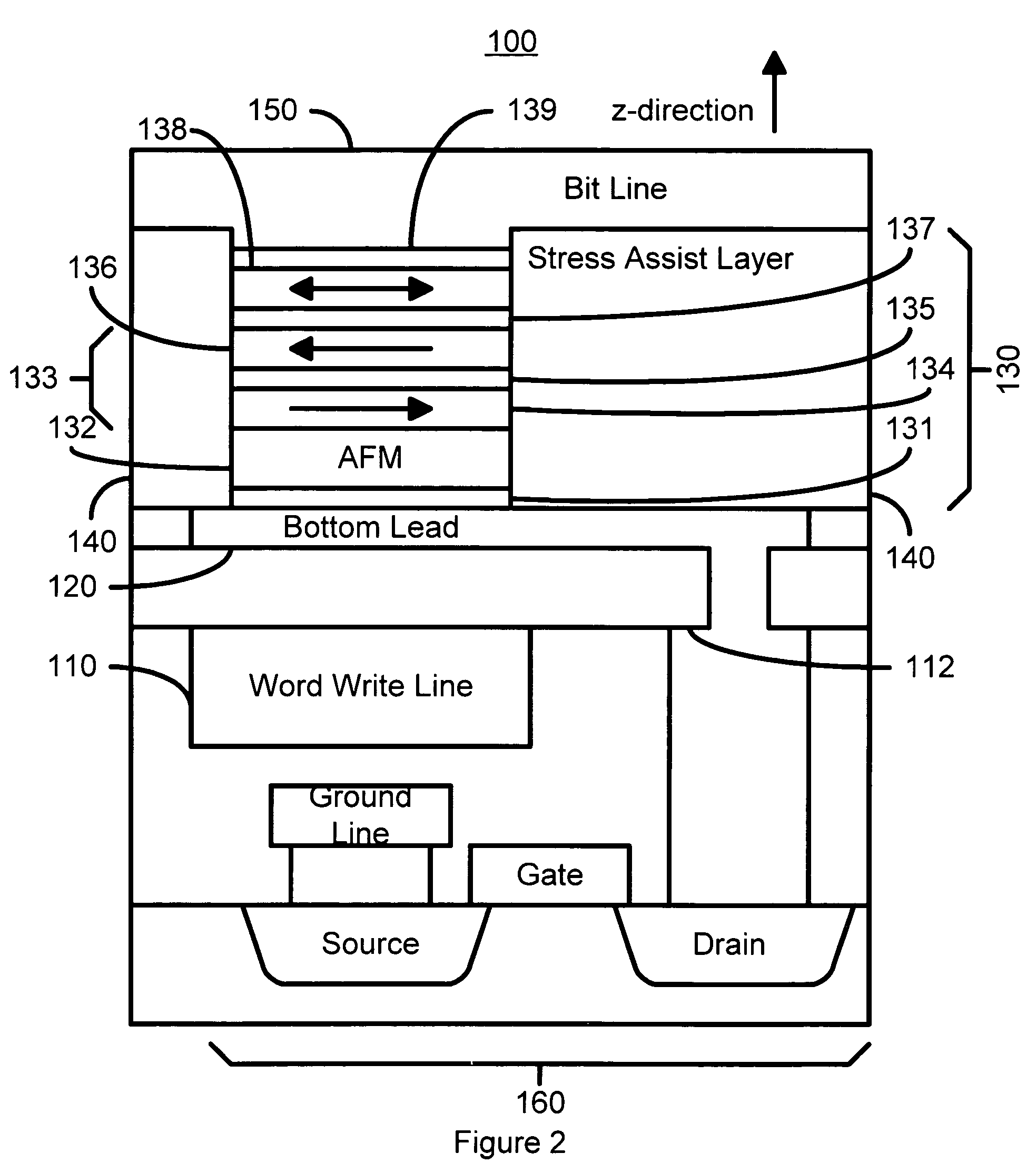
[0043]FIG. 3 is a diagram depicting a portion of a magnetic memory 100′ utilizing stress-assisted switching in accordance with the present invention. The magnetic memory 100′ is analogous to the magnetic memory 100 depicted in FIG. 2. Consequently, components of the magnetic memory 100′ are labeled in an analogous manner. In addition, the materials used for the components of the memory 100′ are preferably the same as for analogous components in the memory 100. However, note that the layer 137′ can be either a barrier layer or a conducting spacer layer, for example made of Cu. Thus, the magnetic element 130′ is preferably either a spin tunneling junction or a spin valve. Note, however, that in an alternate embodiment, other structures could be use for the magnetic element 130′. In addition, the stress-assist layer 140′ is placed below the bottom lead 120′. However, the stress-assist layer 140′ still has the same function. Thus, the stress-assist layer 140′ still causes the magnetic e...

first embodiment

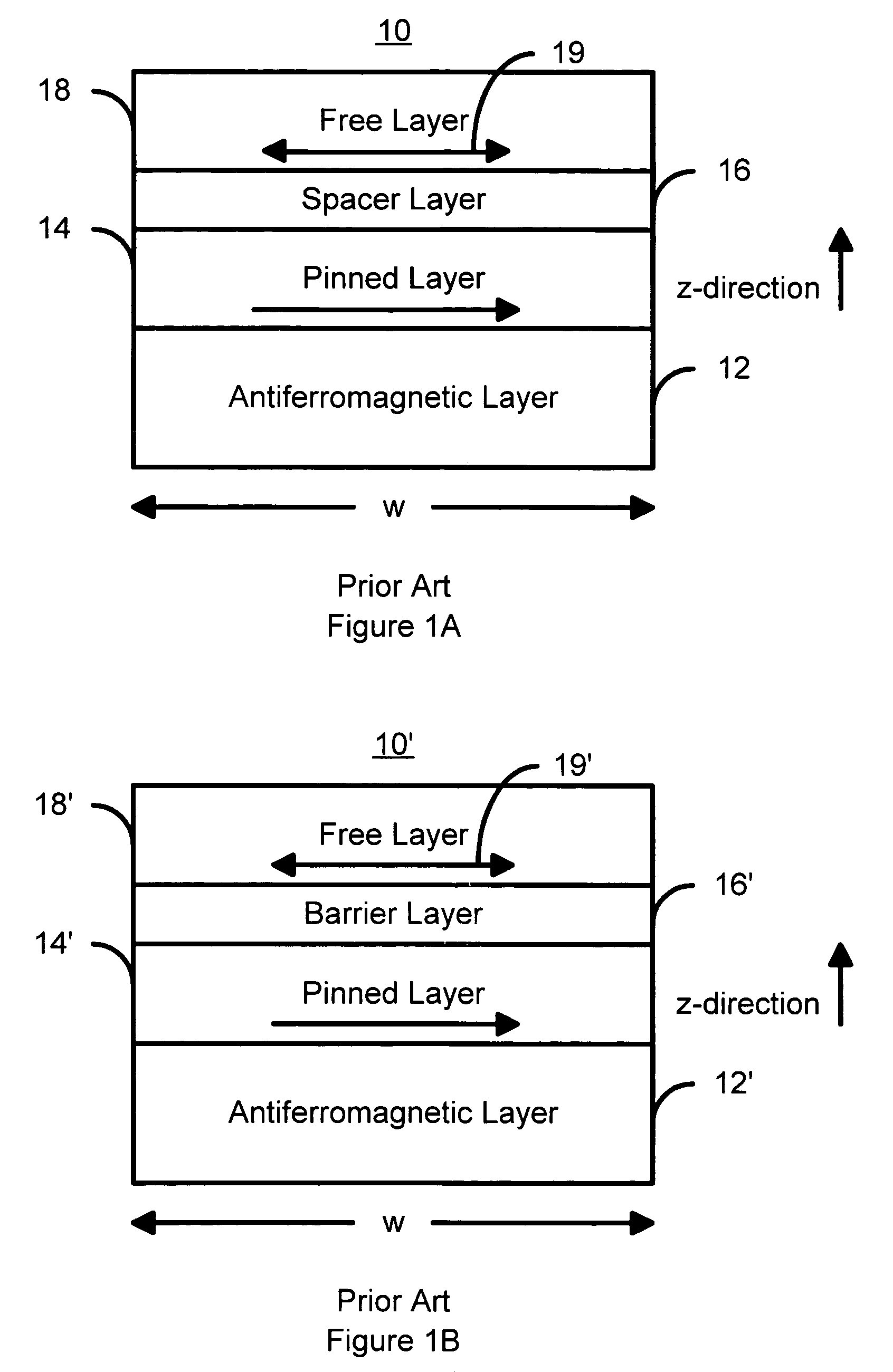
[0046]FIG. 4A is a diagram depicting an alternate switching element 200 in a magnetic element for a magnetic memory utilizing stress assisted switching in accordance with the present invention. The alternate element 200 could replace certain layers in the magnetic element 130 or 130′ including the free layer 138 or 138′, respectively. Thus free layer 202 of magnetic element 200 would be on top of layers 137 or 137′ in the magnetic element 130 or 130′, respectively. The alternate switching element 200 includes a ferromagnetic layer 202, a separation layer 204, a second ferromagnetic layer 206, a spacer layer 208, a pinned layer 210, and an AFM layer 218. The pinned layer 210 is preferably synthetic and, therefore, includes ferromagnetic layers 212 and 216 separated by a nonmagnetic layer 214. The free layer 206 preferably includes materials such as those used for the free layer 138 or 138′. The separation layer 204 preferably includes Cu or CuPt. The separation layer is used to allow...


PUM


Abstract

A method and system for providing a magnetic memory is disclosed. The method and system include providing a plurality of magnetic elements and providing at least one stress-assist layer. Each of the plurality of magnetic elements is configured to be written using spin transfer. The at least one stress-assist layer is configured to exert at least one stress on at least one magnetic element of the plurality of magnetic elements during writing. The reduction of spin-transfer switching current is due to stress exerted by the stress-assist layer on the magnetic elements during writing. Stability of the magnetic memory with respect to thermal fluctuations is not compromised because the energy barrier between the two magnetization states is unchanged once the switching current is turned off.

Description

FIELD OF THE INVENTION[0001]The present invention relates to magnetic memory systems, and more particularly to a method and system for providing an element that employs a stress-assisted spin transfer effect in switching and that can be used in a magnetic memory such as magnetic random access memory (“MRAM”).BACKGROUND OF THE INVENTION[0002]FIGS. 1A and 1B depict conventional magnetic elements 10 and 10′. The conventional magnetic element 10 is a spin valve and includes a conventional antiferromagnetic (AFM) layer 12, a conventional pinned layer 14, a conventional nonmagnetic spacer layer 16 and a conventional free layer 18. Other layers (not shown), such as seed or capping layer may also be used. The conventional pinned layer 14 and the conventional free layer 18 are ferromagnetic. Thus, the conventional free layer 18 is depicted as having a changeable magnetization 19. The conventional nonmagnetic spacer layer 16 is conductive. The AFM layer 12 is used to fix, or pin, the magnetiz...

Claims


Application Information

Patent Timeline
Patent Type & Authority Patents(United States)
IPC IPC(8): H01L29/76G11CG11C11/16G11C17/02H01L21/336H01L21/8246H01L27/22H01L43/08
CPCB82Y10/00B82Y25/00G11C11/16H01F10/3286H01L27/228H01L43/08H01F10/3272H10B61/22H10N50/10G11C11/15G11C17/02
Inventor PAKALA, MAHENDRAHUAI, YIMING
Owner SAMSUNG SEMICON
Why Eureka
Try Eureka