

Semiconductor device manufacturing method
a manufacturing method and semiconductor technology, applied in the direction of semiconductor devices, basic electric elements, electrical appliances, etc., can solve the problems of increasing the demand for smaller device components, and reducing the thickness of the gate oxide film, so as to simplify the dummy gate pattern formation process and reduce the cost
- Summary
- Abstract
- Description
- Claims
- Application Information
AI Technical Summary
Benefits of technology
Problems solved by technology
Method used
Image

Examples
Embodiment Construction
[0030]Below, aspects of the invention are explained, referring to the drawings.
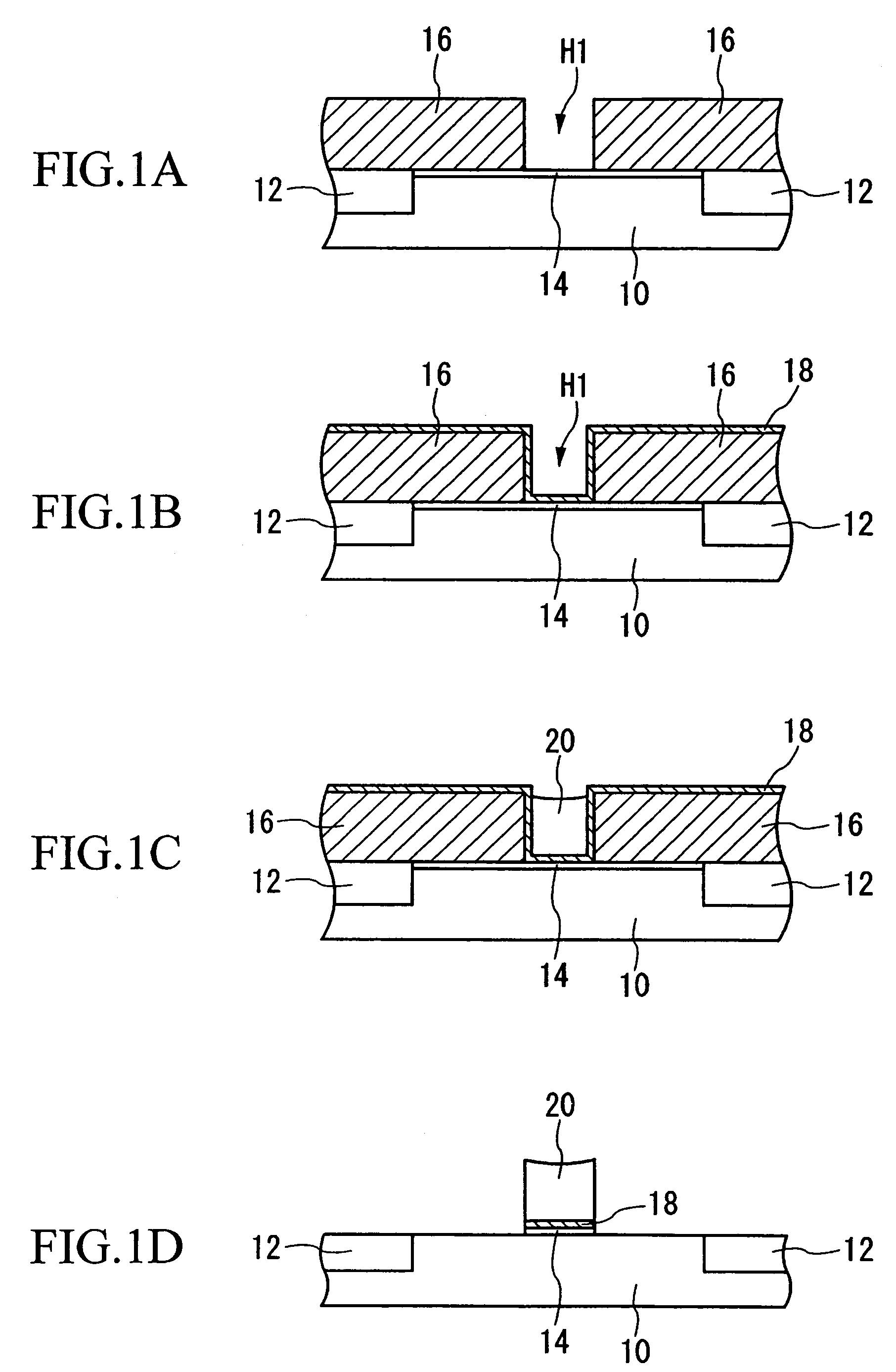
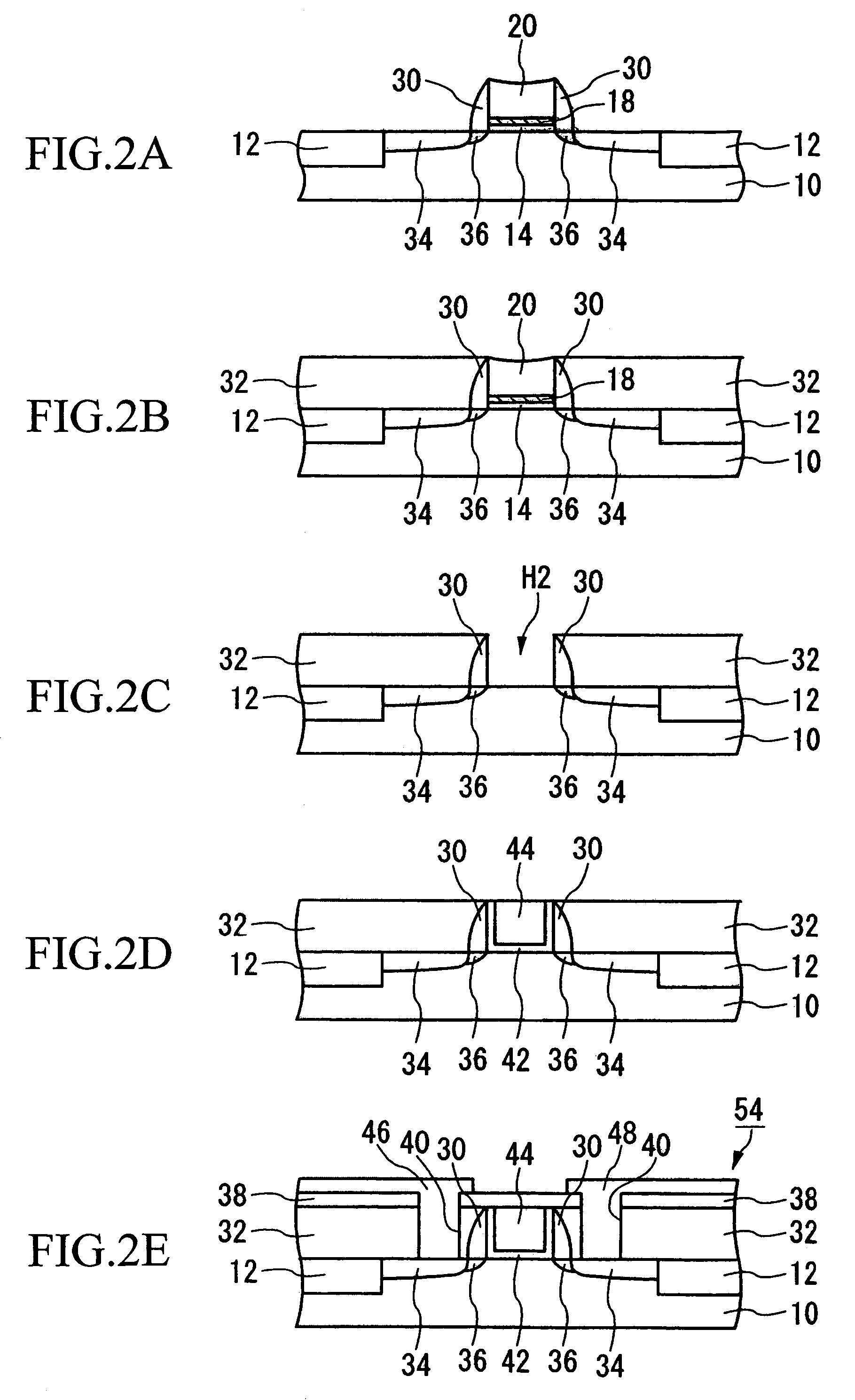
[0031]In one aspect, processes to manufacture a MOSFET having an LDD structure are explained, referring to the drawings. First, the processes to form a dummy gate pattern for use as a mask, when implanting impurities into silicon substrate in a prescribed concentration, are explained in detail. In each of the drawings used in the following explanation, the scales of the various members have been modified appropriately to a size enabling visual identification of the members.
[0032]Method of Formation of Dummy Gate Pattern
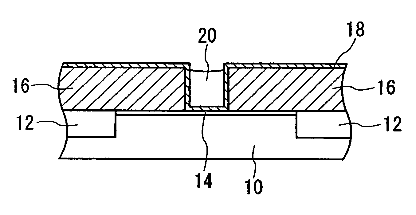
FIGS. 1A to 1D are cross-sectional views showing the processes for formation of a dummy gate pattern in this aspect.
[0033]First, as shown in FIG. 1A, a device separation film 12 is formed, to provide electrical insulation between adjacent devices. Specifically, a reactive ion etching (RIE) method or similar is used to form a shallow trench portion in the silicon substrate 10. This trench po...
PUM
 Abstract
Description
Claims
Application Information