
Method for the producing an integrated circuit bar arrangement, in particular comprising a capacitor assembly, in addition to an integrated circuit arrangement

a technology of integrated circuit and assembly, which is applied in the direction of semiconductor devices, semiconductor/solid-state device details, electrical apparatus, etc., can solve the problems of deterioration in the reliability of electrically conductive connections, parts of electrode layers exposed, and significantly worse electrical characteristics of integrated circuit arrangements, etc., to achieve simple cleaning steps, easy production, and simple method of production

Active Publication Date: 2007-10-23
INFINEON TECH AG
View PDF16 Cites 13 Cited by
  • Summary
  • Abstract
  • Description
  • Claims
  • Application Information

AI Technical Summary

Benefits of technology

This approach simplifies the production process, reduces the risk of damage to the dielectric layer, and improves the electrical characteristics of the integrated circuit by avoiding oxidation and underetching, resulting in a more reliable and efficient manufacturing method.

Problems solved by technology

However, this has the disadvantage that, during the removal of the resist, parts of the electrode layer are exposed and are thus attacked by the chemical processes which are used to remove the resist.
If the reaction products which are produced during removal of the resist on the electrode layer are not removed completely, then this leads to high contact resistances, resulting in a deterioration in the reliability of the electrically conductive connections.
Underetching thus occurs during removal of the reaction products, making the electrical characteristics of the integrated circuit arrangement considerably worse.

Method used


Image

  • Method for the producing an integrated circuit bar arrangement, in particular comprising a capacitor assembly, in addition to an integrated circuit arrangement
  • Method for the producing an integrated circuit bar arrangement, in particular comprising a capacitor assembly, in addition to an integrated circuit arrangement
  • Method for the producing an integrated circuit bar arrangement, in particular comprising a capacitor assembly, in addition to an integrated circuit arrangement

Examples


Embodiment Construction

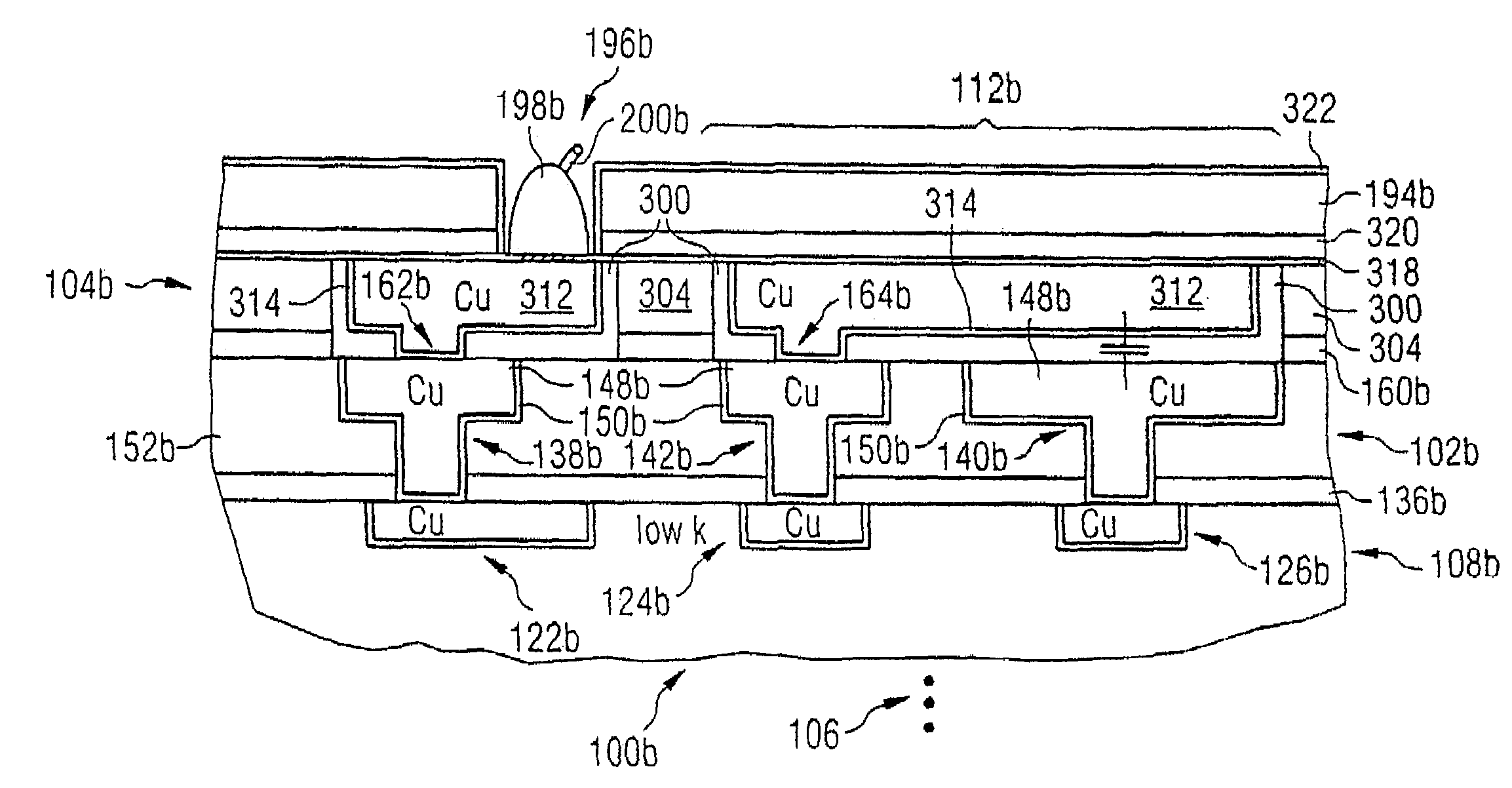
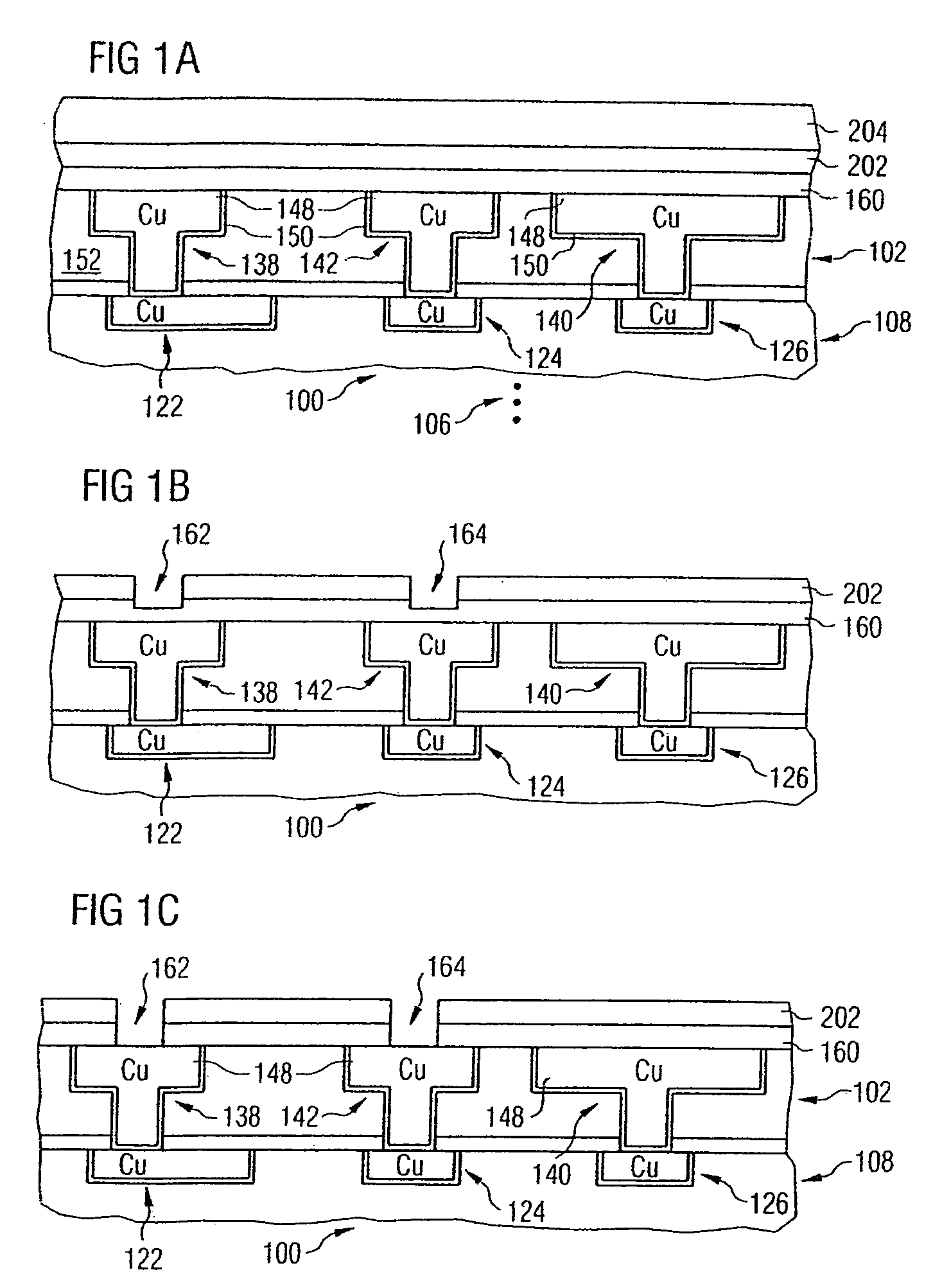
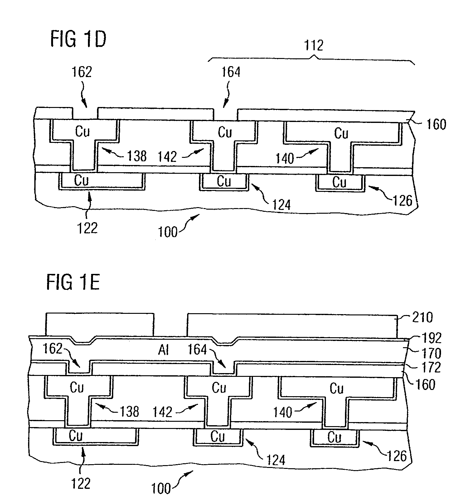
[0034]FIG. 1F shows a circuit arrangement 100 with a penultimate metallization layer 102 and a last metallization layer 104. A metallization layer 108 is located under the penultimate metallization layer 102. Metallization layers 106 which are arranged under the metallization layer 108, and a substrate of the circuit arrangement 100, are indicated by dots.

[0035]FIG. 1F shows a bonding connection 110 and a linear capacitor 112 as examples of components which may be arranged in the two uppermost metallization layers 102 and 104.

[0036]The metallization layer 108 contains as the insulating material a material having a low dielectric constant k (BLOK—Barrier LOw K), for example SILK (Silicon LOw K), that is to say for example porous silicon dioxide 120. Alternatively, FSG (Fluoride Silicate Glass) is used as the insulating material in the metallization layer 108. In the area of the bonding connection 110, the metallization layer 108 contains an interconnect 122. The interconnect 122 cont...


PUM


Abstract

A method for production of an integrated circuit arrangement which contains a capacitor. A dielectric layer is structured with the aid of a two-stage etching process, and with the aid of a hard mask. In the case of an electrically insulating hard mask, the hard mask is removed again. In the case of an electrically conductive hard mask, parts of the hard mask may remain in the circuit arrangement.

Description

[0001]This application is a continuation of PCT patent application No. PCT / EP03 / 014974, filed Dec. 31, 2003, which claims the benefit of priority to German Patent Application DE 10301243.5, filed Jan. 15, 2003, both of which are incorporated herein by reference.TECHNICAL FIELD[0002]The invention relates to integrated circuit arrangements and to methods for production of integrated circuits.BACKGROUND[0003]One method of producing an integrated circuit arrangement includes the application of a dielectric layer to an electrode layer which contains at least one electrode. Followed by application of a resist layer, structuring of the dielectric layer, and removing residues of the resist layer.[0004]At a temperature of 20° C., the dielectric layer has an electrical resistivity of, for example, more than 1010 Ωcm or even 1016 Ωcm. By way of example, silicon dioxide is used as the material for the dielectric layer. However, materials with a dielectric constant of more than 3.9 are also used...

Claims


Application Information

Patent Timeline
Patent Type & Authority Patents(United States)
IPC IPC(8): H01L21/4763H01L23/522H01L23/532
CPCH01L23/5223H01L24/05H01L23/53238H01L2224/48463H01L2224/04042H01L2224/02166H01L2924/00H01L2924/14
Inventor BARTH, HANS-JOACHIMHOLZ, JURGEN
Owner INFINEON TECH AG
Learn More