Electrostatic discharge protection device for digital circuits and for applications with input/output bipolar voltage much higher than the core circuit power supply

a protection device and digital circuit technology, applied in the field of transistors, can solve the problems of increasing the reliability problems of cmos devices, reducing the lifetime of ics, and being more sensitive to damag

Inactive Publication Date: 2007-10-23
UNIV OF CENT FLORIDA RES FOUND INC +1
View PDF12 Cites 56 Cited by
  • Summary
  • Abstract
  • Description
  • Claims
  • Application Information

AI Technical Summary

Benefits of technology

[0015]In accordance with the present teachings, there is a tunable thyristor device without a gate for the design of ESD protection at I / O pads and as a supply clamp for CMOS circuits. The device is designed using two different structures and also has complementary versions, n- and p-type. The disclosed protection device will be referred to hereinafter as a substrate triggered thyristor (STT). This device can be classified in two types: 1) n-and p-type double-substrate-triggered thyristor (n- and p-type DSTT) and 2) n- and p-type single- substrate-triggered-thyristor (n- and p-type SSTT). The present teachings provide a versatile, space-efficient, and reliable ESD protection device for a more robust implementation of ESD protection systems in advanced sub-micron CMOS technologies.

Problems solved by technology

The technology advance has in turn increased the CMOS devices' reliability problems, reducing the lifetime of the ICs and making them more sensitive to damage in the early steps of the production and assembly processes.
The IC's sensitivity to Electrostatic Discharge (ESD) is one of the most critical reliability problems in the semiconductor industry.
The process results in an abrupt peak of current that can cause severe damage in the microchip.
There are important complications though.
The former ESD solutions typically cannot be readily scaled-down like the other components of an IC core circuit or migrated with the same sizes without paying an ESD performance penalty.
Nevertheless, these process improvements usually make the core circuit even more sensitive, and devices previously used for ESD protection may no longer be self-protected.
Moreover, even increasing the size of the traditional protection structures to levels comparable with the core circuit dimensions does not guarantee that the ESD requirements are met.
This condition creates a bottleneck for sub-micron IC development and diminishes the potential advantages of the CMOS scaling.
The SCRs meet this characteristic, but the trigger voltage is very high and severe damage may occur in a sub-micron core circuit before the protection device triggers.
The LVTSCR has been used in the previous art for CMOS IC ESD protection, but it has the disadvantage that the holding voltage is very low and causes latchup problems in circuits where the I / O pad operation voltage is higher than about 1.2V.
However, these devices are highly dependent on the rise time and decay time of the ESD event as well as on temperature fluctuations.
Results show that different versions of devices with floating gates exhibit characteristics that may cause a misleading interpretation of the device performance.
In a floating gate device, the conduction characteristics are unpredictably modified by the gate conditions.
The leakage current through the channel of the protection device increases abruptly, leading to a circuit latchup, failure of the ESD protection, and / or further damage of the protected IC.

Method used


Image

  • Electrostatic discharge protection device for digital circuits and for applications with input/output bipolar voltage much higher than the core circuit power supply
  • Electrostatic discharge protection device for digital circuits and for applications with input/output bipolar voltage much higher than the core circuit power supply
  • Electrostatic discharge protection device for digital circuits and for applications with input/output bipolar voltage much higher than the core circuit power supply

Examples


Embodiment Construction

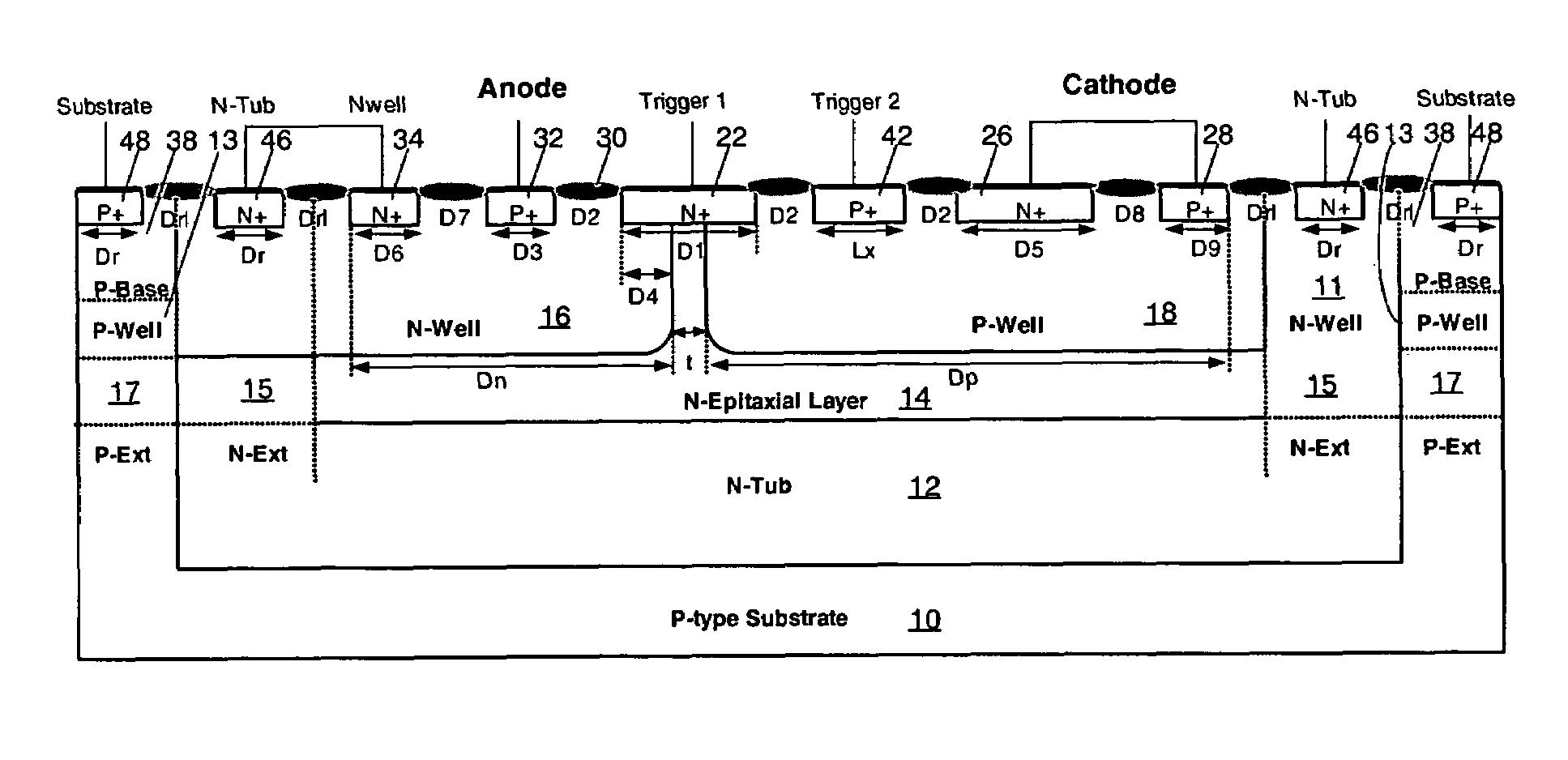
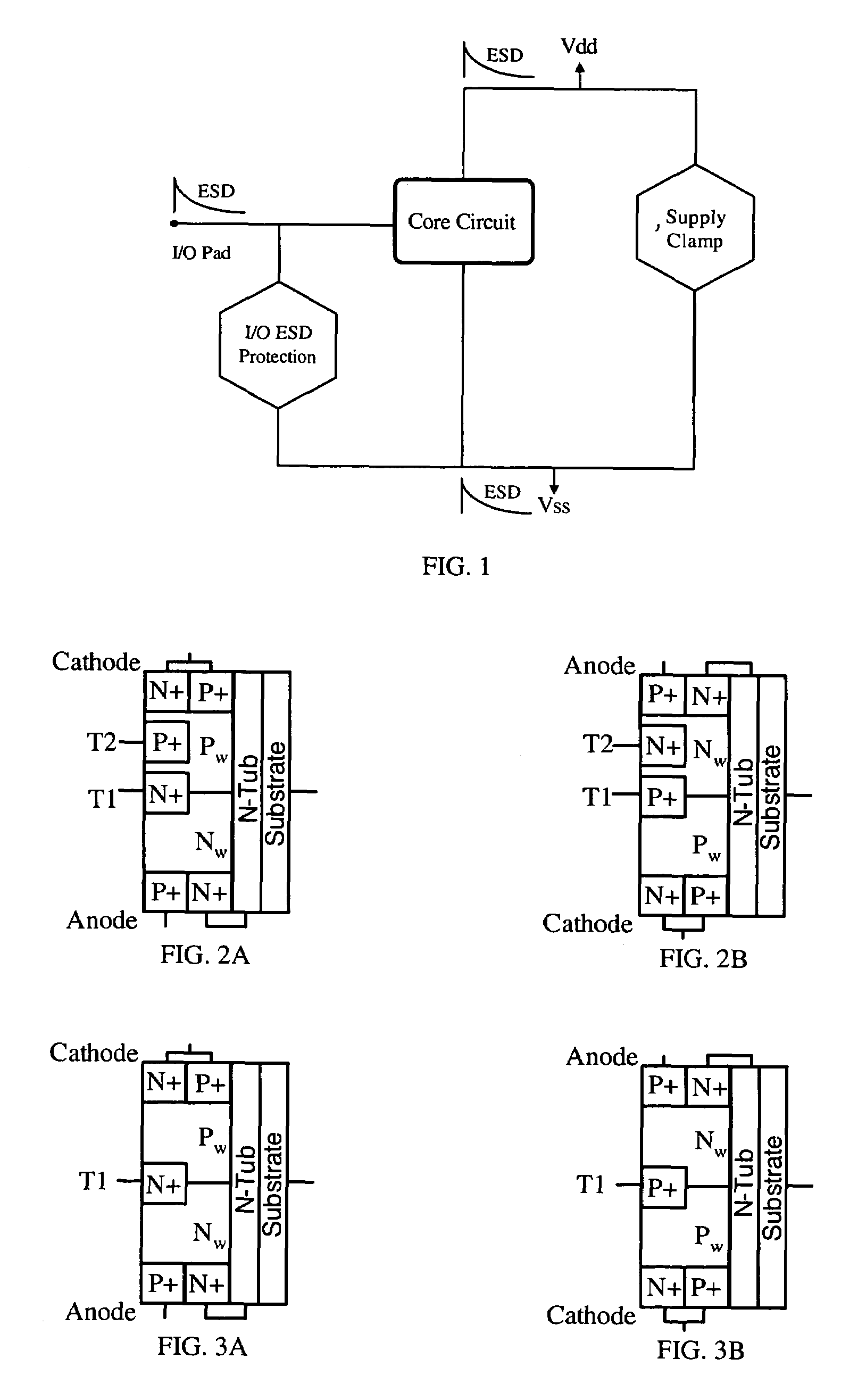
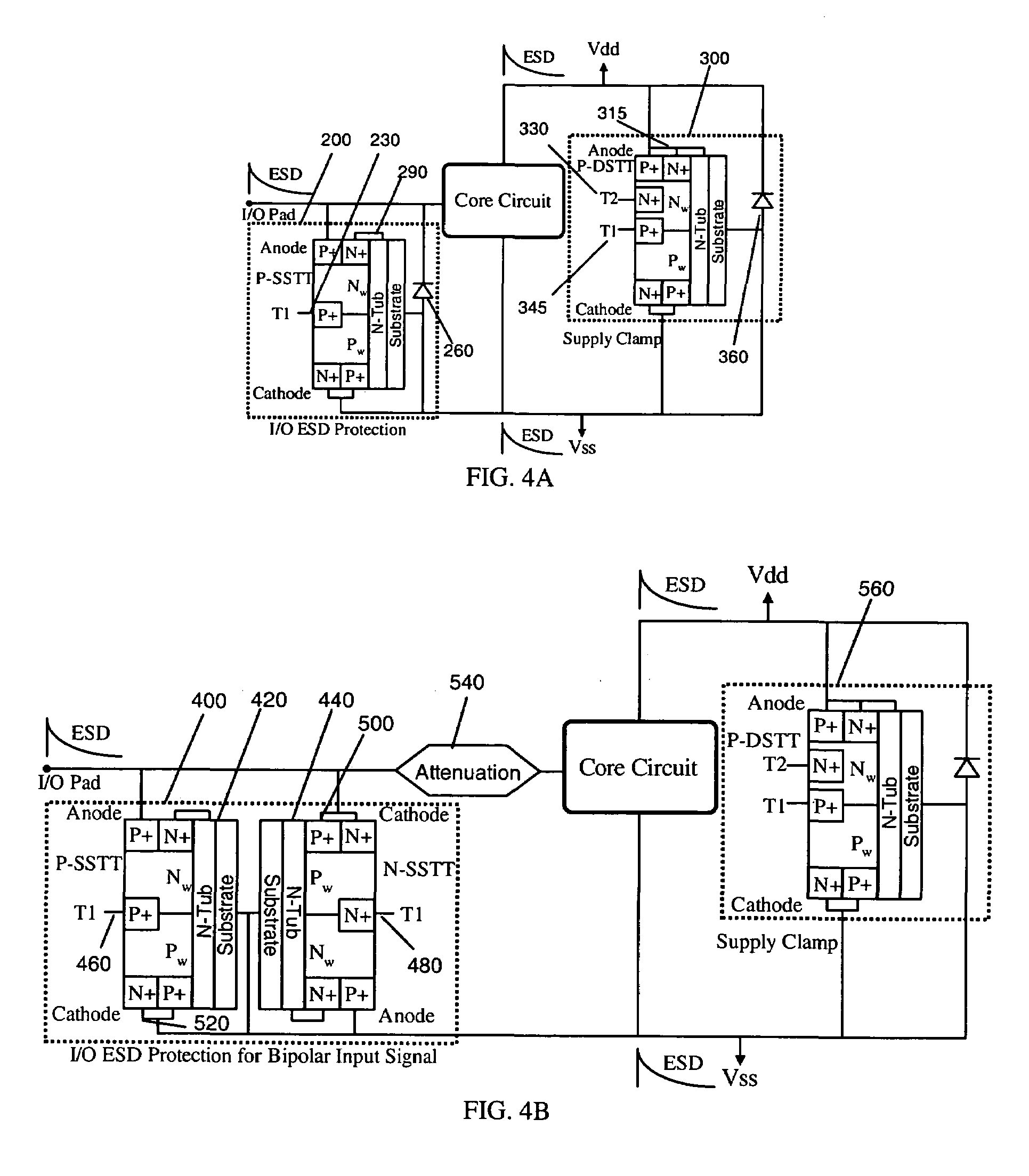
[0040]In the following description, reference is made to the accompanying drawings that form a part thereof, and in which is shown by way of illustration specific exemplary embodiments in which the invention may be practiced. These embodiments are described in sufficient detail to enable those skilled in the art to practice the invention and it is to be understood that other embodiments may be utilized and that changes may be made without departing from the scope of the invention. The following description is, therefore, not to be taken in a limited sense.

[0041]Notwithstanding that the numerical ranges and parameters setting forth the broad scope of the invention are approximations, the numerical values set forth in the specific examples are reported as precisely as possible. Any numerical value, however, inherently contains certain errors necessarily resulting from the standard deviation found in their respective testing measurements. Moreover, all ranges disclosed herein are to be...


PUM


Abstract

An electrostatic discharge (ESD) device and method is provided. The ESD device can comprise a substrate doped to a first conductivity type, an epitaxial region doped to the second conductivity type, and a first well doped to the first conductivity type disposed in the substrate. The first well can comprise a first region doped to the first conductivity type, a second region doped to a second conductivity type, and a first isolation region disposed between the first region and the second region. The ESD device can also comprise a second well doped to a second conductivity type disposed in the substrate adjacent to the first well, where the second well can comprise a third region doped to the first conductivity type, a fourth region doped to the second conductivity type, and a second isolation region disposed between the third region and the fourth region. Still further, the ESD device can include a first trigger contact and second trigger contact comprising highly doped regions of either conductivity type, the first trigger contact disposed at a junction between the first well and the second well, and the second trigger contact disposed at either well.

Description

CROSS-REFERENCE TO RELATED APPLICATIONS[0001]This application claims priority to U.S. Provisional Patent Application Ser. No. 60 / 643,692 filed on Jan. 12, 2005, the disclosure of which is incorporated by reference in their entirety.FIELD OF THE INVENTION[0002]The subject matter of this application relates to transistors. More particularly, the subject matter of this application relates to on-chip Electrostatic Discharge (ESD) Protection in Complementary Metal Oxide Semiconductor (CMOS) Integrated Circuits (ICs).BACKGROUND OF THE INVENTION[0003]Complementary Metal Oxide Semiconductor (CMOS) technology has for many years led the semiconductor industry in the fabrication of reliable and low-cost Integrated Circuits (ICs). The remarkable development of this technology is continuously evolving to fabricate smaller and faster devices for Very Large Scale Integration (VLSI) systems. The technology advance has in turn increased the CMOS devices' reliability problems, reducing the lifetime o...

Claims


Application Information

Patent Timeline
Patent Type & Authority Patents(United States)
IPC IPC(8): H01L23/62
CPCH01L27/0262H01L29/7436H01L2924/0002H01L2924/00
Inventor SALCEDO, JAVIER A.LIOU, JUIN J.BERNIER, JOSEPH C.WHITNEY, DONALD K.
Owner UNIV OF CENT FLORIDA RES FOUND INC
Why Eureka
Try Eureka