Display device, method of driving same and electronic device mounting same

a technology of liquid crystal display device and drive method, which is applied in the direction of static indicating device, non-linear optics, instruments, etc., can solve the problems of inability to apply the foregoing driving method to the matrix-type liquid crystal display device, inability to apply the foregoing driving method to the display device which deals with complicated information, and inability to achieve the effect of reducing power consumption, suppressing flicker noise, and significantly reducing power consumption

Inactive Publication Date: 2007-10-23
SHARP KK
View PDF20 Cites 129 Cited by
  • Summary
  • Abstract
  • Description
  • Claims
  • Application Information

AI Technical Summary

Benefits of technology

[0032]According to the foregoing arrangement, an auxiliary capacitance is formed in an area such that a capacitive bond is not generated between the electrode of the auxiliary capacitance according to a predetermined electric capacitance and the scanning signal line. Therefore, with the foregoing structure, by arranging such that at a rewriting frequency at which a charge in the liquid crystal capacitance CLC, i.e., the screen of the display element is rewritten is set to be not more than 30 Hz by the frequency setting means, the problem with the conventional case of forming the auxiliary capacitance in the Cs-on-gate structure, i.e., fluctuation in potential of the pixel electrode of the electric capacitance due to fluctuation in potential of the scanning signal lines such as a scanning signal lines in one line above can be prevented.
[0044]Therefore, the matrix-type display device which permits required power consumption to be significantly reduced, and in which flicker noise is suppressed to a sufficiently low level can be realized.

Problems solved by technology

The foregoing power consumption reducing techniques are preferable for the segment display type liquid crystal display devices, and figurative performances are therefore limited to the display of simple numerals or pictographs.
It is therefore not possible to apply the foregoing techniques to the display devices which deal with complicated information, such as personal computers, portable information terminals, etc.
It is also difficult of apply the foregoing driving method to the matrix-type liquid crystal display devices.
It is therefore not possible to ensure a stable display.
For the matrix-type liquid crystal display of a simple multiplex driving system, although a power consumption is relatively small, for example, in the range of from 10 mW to 15 mW for the size of type 2, the problems arise in basic display performances, such as insufficient brightness, contrast, response speed.
In contrast, for the matrix-type liquid crystal display of active driving system adopting TFTs, etc., although sufficient basic display quality can be ensured as to brightness, contrast, response speed, etc., the power consumption within the range of from 100 mW to 150 mW is required for the size type 2 it, and it is not possible to achieve a reduction in power consumption to the satisfactory level.
In the liquid crystal display device of the active matrix display system, not only that the rewriting is performed at high frequency, but also that the voltage polarity of the data signal is reversed per one scanning signal line, resulting in an increase in power consumption of a scanning signal driver and a data signal driver.
As a result, flicker noise occurred.
As can be seen from the result of the experiment, it was found that when merely reducing the rewriting frequency in the Cs-on-gate structure to reduce the low power consumption, deterioration of display quality cannot be avoided.
According to the method of Japanese Laid-Open Patent Publication No. 107563 / 1997, throughout the field period, any of liquid crystal panels is driven, and the required power consumption may not be increased but cannot be reduced.
When applying this method to the system for directly seeing the liquid crystal panel, flicker noise is liable to be perceptible.
Furthermore, flicker noise generates every line even when multi-field driving, and therefore flicker noise is recognized even when the flicker noise is cancelled out between adjoining lines, which leads to a significant deterioration in visibility.
Furthermore, an expected reduction in driving frequency is very small, and a sufficient reduction in power consumption cannot be achieved.
In the multi-field driving system, one screen is divided into a plurality of sub fields, and scanning is performed very other lines or every other plural lines, and therefore, it is required to read out signals corresponding to the scanning signal line to be driven after once storing the image in the frame memory, and therefore the structure of the circuit inevitably complicated.
As a result, the peripheral circuit becomes larger in size, and a manufacturing cost increases.
Furthermore, according to the method disclosed in Japanese Laid-Open Patent Publication No. 342148 / 1994 (Tokukaihei 6-342148), a ferroelectric liquid crystal is basically for the binary value (black-and-white), and a gradation display cannot be achieved, and a natural display cannot be achieved.
Furthermore, in order to arrange ferroelectric liquid crystals in a panel, an advanced technique is required for preparing panels, and thus it is difficult to adopt it in practical applications.
Therefore, the foregoing method has not yet being used in practical applications.
In the method of driving a conventional matrix-type display device, it was not possible to realize a reduction in power consumption while ensuring basic display characteristics such as brightness, contrast, response speed, gradation, etc.
Furthermore, in the conventional method of driving the matrix-type liquid crystal display device, it is not possible to realize both reduction in power consumption to a sufficient level and a high quality display device without flicker noise at the same time.

Method used


Image

  • Display device, method of driving same and electronic device mounting same
  • Display device, method of driving same and electronic device mounting same
  • Display device, method of driving same and electronic device mounting same

Examples


first embodiment

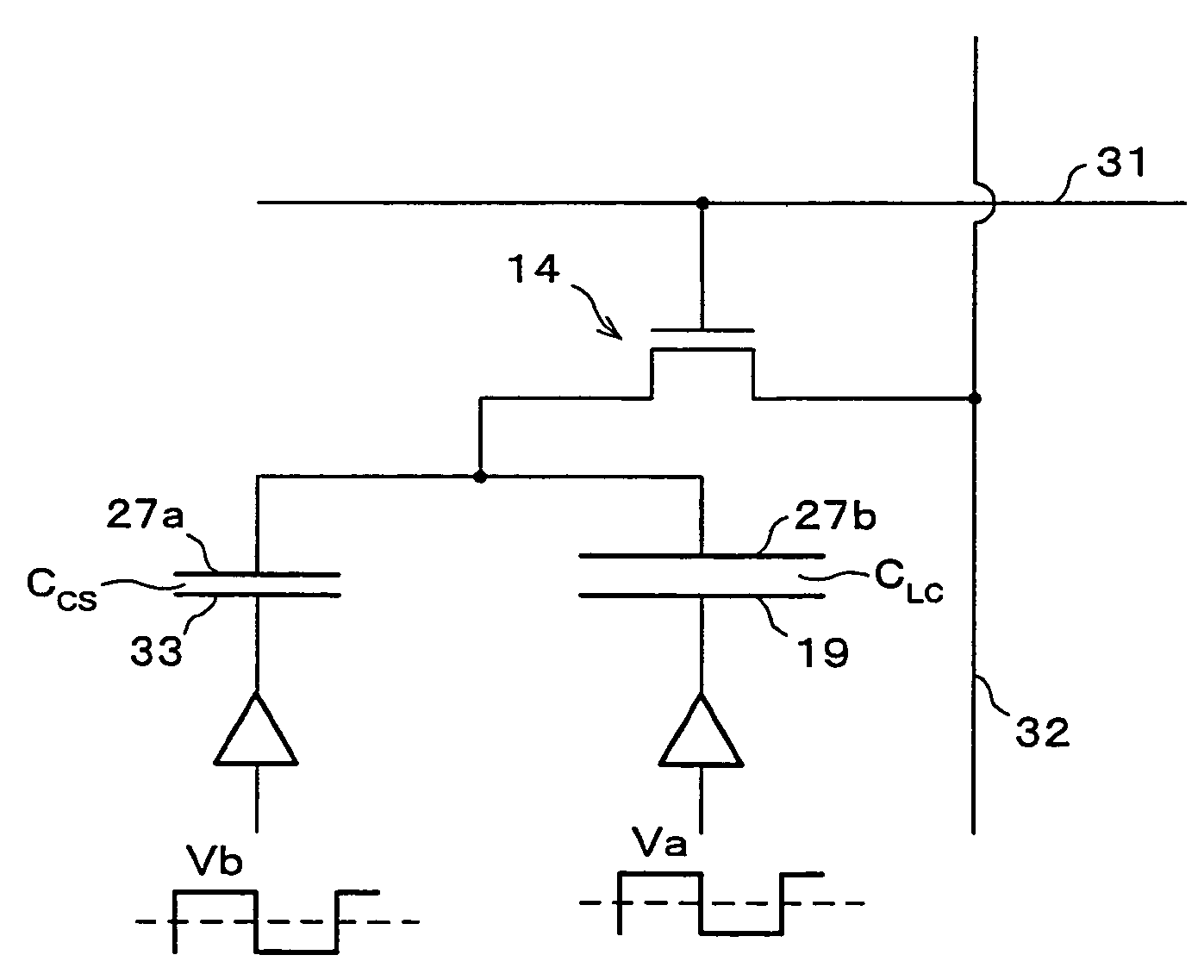
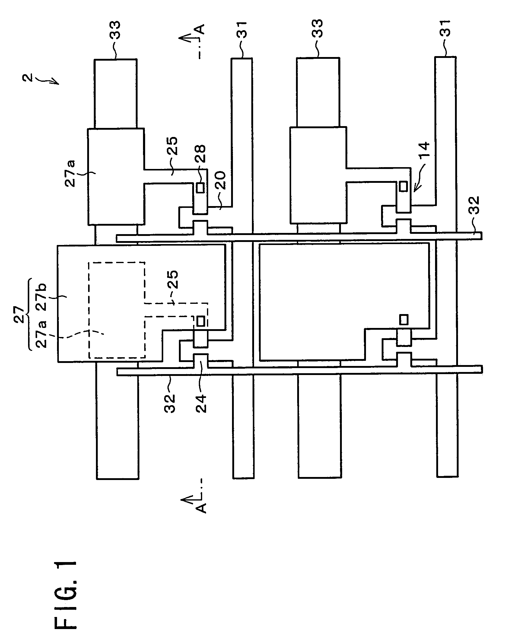
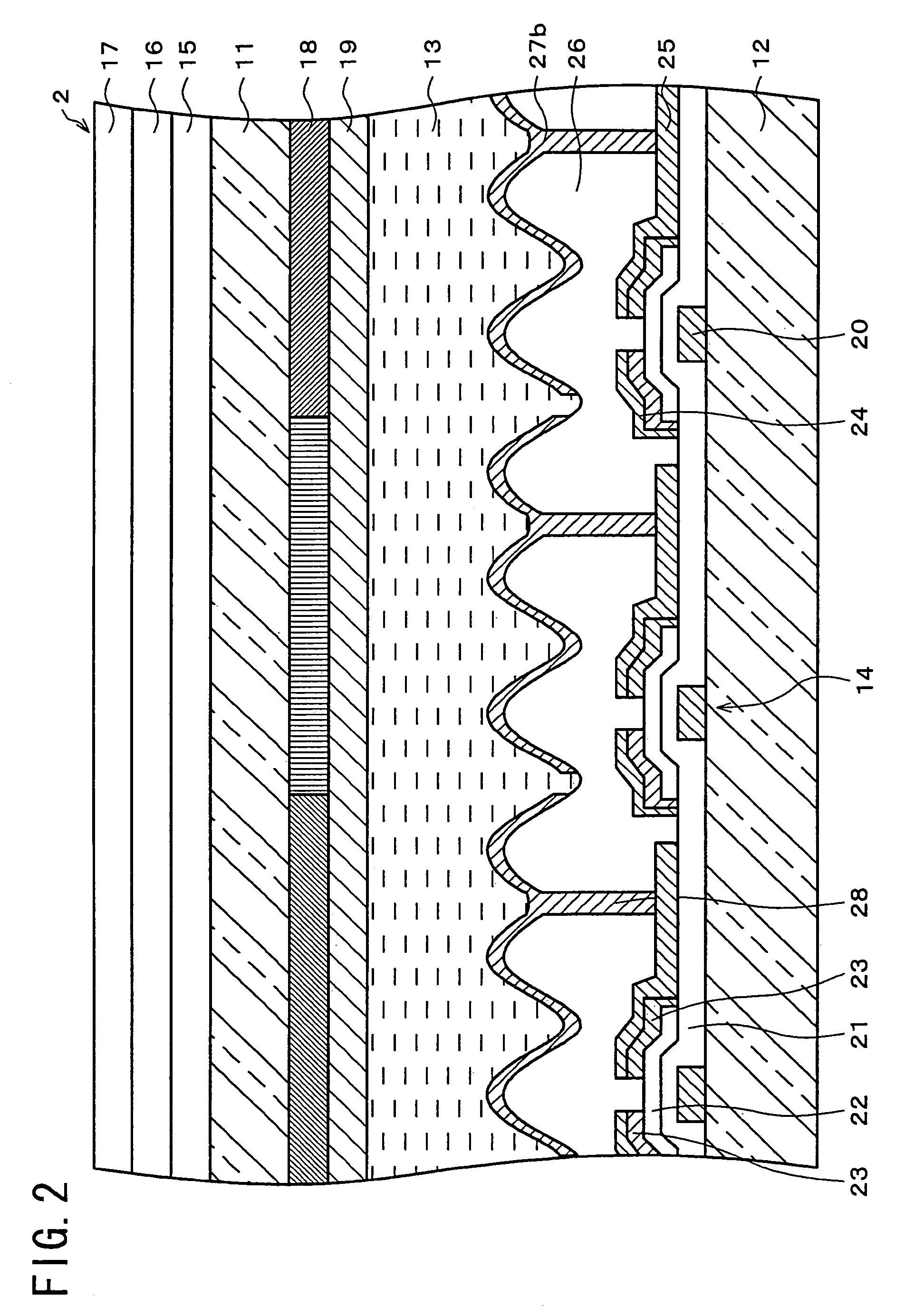
[0103]The following descriptions will discuss one embodiment provided with a display device of the present invention in reference to FIGS. 1 to 11.

[0104]The inventors of the present application tried to find out a cause of flicker noise generated when driving the liquid crystal display device having a Cs-on-gate structure with a rewriting frequency of 30 Hz or below, and have found to be the following.

[0105]In the case of a so-called Cs-on-gate structure wherein auxiliary capacitive electrodes of pixels in a liquid crystal display element having an active element are formed on a scanning signal line in one line above the pixels, the pixel electrode potential of the pixels largely fluctuate with an application of scanning signals onto the scanning signal line in one line above the pixels. Generally, when adopting the rewriting frequency of 30 Hz or higher, a response of liquid crystal molecules due to fluctuation in pixel electrode potential is averaged and is therefore not perceptib...

second embodiment

[0165]The following descriptions will discuss still another embodiment of the display device of the present invention in reference to FIG. 12 through FIG. 19. For ease of explanation, members (structures) having the same functions as those shown in the drawings pertaining to the first embodiment above will be given the same reference symbols, and explanation thereof will be omitted here.

[0166]The display device of the present embodiment has the same structure as the liquid crystal display device 1 except that a liquid crystal panel 51 shown in FIGS. 12 and 13 is adopted as a display element (liquid crystal display element) in replace of the liquid crystal panel 2 of the first embodiment as explained in reference to FIG. 3.

[0167]FIG. 13 shows the cross-sectional view of the liquid crystal panel 51 which is a cross section of the portion along a line B-B of FIG. 12 to be described layer. The liquid crystal panel 51 is an active matrix liquid crystal panel of reflective type, and the b...

third embodiment

[0190]The following descriptions will discuss still another embodiment of the display device of the present invention in reference to FIG. 21 and FIG. 22. For ease of explanation, members (structures) having the same functions as those shown in the drawings pertaining to the first and second embodiments above will be given the same reference symbols, and explanation thereof will be omitted here.

[0191]The display device in accordance with the present embodiment is a liquid crystal display device which serves both as a transmissive mode and a reflective mode wherein the liquid crystal panel 2 in the liquid crystal display device 1 as explained using FIG. 3 in the first embodiment is replaced with the liquid crystal panel 1 illustrated in FIG. 21 and FIG. 22. As illustrated in FIG. 21 which is a cross-sectional view of the portion along a line D-D of FIG. 22, the liquid crystal panel 91 differs from the liquid crystal panel 91 in that the anti-reflection film 17 and the color filter 18...


PUM


Abstract

A liquid crystal panel (2) includes scanning signal lines (31) for supplying scanning signals to gate electrodes (20) of TFTs (14), and data signal lines (32) for supplying data signals to data electrodes (24) of TFTs. The liquid crystal panel further includes auxiliary capacitive electrode pads (27a) for use in forming auxiliary capacitance and an auxiliary capacitive lines (33) so as not to generate a capacitive bond with the scanning signal lines. The liquid crystal panel is driven at a rewriting frequency of a screen of not more than 30 Hz. As a result, the liquid crystal panel can be driven at a low consumption power while maintaining a desirable display quality of the liquid crystal panel.

Description

[0001]This application is a divisional of co-pending U.S. application Ser. No. 09 / 856,926, filed May 29, 2001, which was a National Stage Filing of PCT Application No. PCT / JP01 / 03543, filed Apr. 24, 20001, the teachings of all being incorporated herein by reference.TECHNICAL FIELD[0002]The present invention relates to techniques which realize a display device of reduced power consumption.BACKGROUND OF THE INVENTION[0003]Recent years have seen a rapid increase in demands for liquid crystal devices in various applications such as word processors, lap-top personal computers, pocket televisions. Particularly, reflective-type liquid crystal device, which displays by reflecting an incident light from the exterior, has been viewed with interest for their beneficial features as to small-power consumption, thinness, and light weight as achieved by eliminating the need of backlight.[0004]Conventional reflective-type liquid crystal devices can be classified into the following three systems: th...

Claims


Application Information

Patent Timeline
Patent Type & Authority Patents(United States)
IPC IPC(8): G09G3/36G02F1/1368G02F1/1362G09G3/20G09G3/32
CPCG02F1/136213G09G3/3258G09G3/3614G09G3/3648G09G3/3655G09G3/3677G09G3/3688G02F1/133553G09G2360/18G09G3/2092G09G3/3208G09G3/3266G09G2300/0426G09G2300/0819G09G2300/0823G09G2300/0876G09G2310/0254G09G2310/027G09G2310/065G09G2310/08G09G2320/0209G09G2320/0247G09G2330/021G02F1/133555
Inventor TSUDA, KAZUHIKOSHIMIZU, MASAHIRONAKAMURA, HISAKAZUKUMADA, KOUJIOHTA, TAKASHIGE
Owner SHARP KK
Why Eureka
Try Eureka