Display device

a display device and active matrix technology, applied in the field of display devices, can solve problems such as the degradation of display quality, and achieve the effects of reducing the number of display devices, simple configuration, and efficient suppression of lateral crosstalk

Inactive Publication Date: 2013-11-21
SHARP KK
View PDF4 Cites 2 Cited by
  • Summary
  • Abstract
  • Description
  • Claims
  • Application Information

AI Technical Summary

Benefits of technology

[0059]According to the first aspect of the present invention, the potential of the auxiliary capacitance line is corrected by an output signal from the differential amplifier. Therefore, the time until the potential of the auxiliary capacitance line fluctuated at the time of writing a data signal recovers to the original potential becomes shorter than that in the conventional technique, so that a fluctuation in the pixel potential caused by the potential fluctuation in the auxiliary capacitance line does not occur. It is sufficient to provide one differential amplifier. As a result, a lateral crosstalk can be suppressed with the simple configuration.
[0060]According to the second aspect of the present invention, a change-over switch is controlled by the potential of a scanning signal line. Therefore, only the auxiliary capacitance line in which a potential fluctuation occurs is corrected and, further, it is unnecessary to separately use a signal for controlling the change-over switch. Consequently, the lateral crosstalk can be efficiently suppressed with the simple configuration.
[0061]According to the third aspect of the present invention, in the case where there are three or more kinds of potentials to be applied to an auxiliary capacitance line, without performing special designing to the auxiliary capacitance line drive circuit, effects similar to those of the second aspect of the present invention can be produced.
[0062]According to the fourth aspect of the present invention, since the input-end-side switching element is controlled by the potential of the scanning signal line, it is unnecessary to separately use a signal for controlling the input-end-side switching element. Consequently, effects similar to those of the third aspect of the present invention can be produced with the simpler configuration.
[0063]According to the fifth aspect of the present invention, the potential of the auxiliary capacitance line corresponding to a scanning signal line which is in the non-selection state is not influenced by the potential of the auxiliary capacitance line corresponding to a scanning signal line which is in the selection state. Thus, a lateral crosstalk can be suppressed more efficiently.
[0064]According to the sixth aspect of the present invention, an output-end-side switching element is controlled by the potential of the scanning signal line, so that it is unnecessary to separately use a signal for controlling the output-end-side switching element. Consequently, effects similar to those of the fifth aspect of the present invention can be produced with the simpler configuration.

Problems solved by technology

Due to this, the conventional liquid crystal display device using the method of performing the polarity inversion driving by changing the potential of a corresponding auxiliary capacitance line after completion of the selection period of each scanning signal line has a problem such that a crosstalk in the lateral direction (hereinbelow, called “lateral crosstalk”) occurs and display quality deteriorates.

Method used


Image

  • Display device
  • Display device
  • Display device

Examples


first embodiment

1. First Embodiment

[0114]

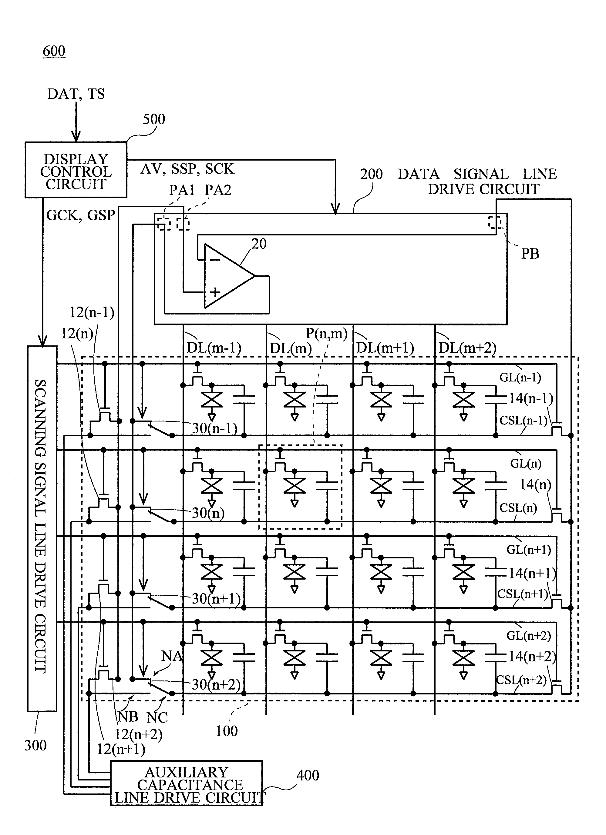
[0115]FIG. 1 is a circuit diagram illustrating an electrical configuration of a liquid crystal display device according to a first embodiment of the present invention. The same reference numerals are designated to the same elements as those of the conventional liquid crystal display device 690 in components of the embodiment and their description will not be repeated. As illustrated in FIG. 1, a liquid crystal display device 600 of the embodiment has a display panel 100, a data signal line drive circuit 200, the scanning signal line drive circuit 300, the auxiliary capacitance line drive circuit 400, and the display control circuit 500. Any or all of the data signal line drive circuit 200, the scanning signal line drive circuit 300, the auxiliary capacitance line drive circuit 400, and the display control circuit 500 are, for example, installed as ICs (Integrated Circuits) on the TFT substrate of the display panel 100. Any or all of the data signal line driv...

second embodiment

2. Second Embodiment

[0138]

[0139]FIG. 8 is a circuit diagram illustrating an electrical configuration of a liquid crystal display device 610 according to a second embodiment of the present invention. The liquid crystal display device 610 of the embodiment has a configuration similar to that of the liquid crystal display device 600 of the first embodiment except for having capacitors 16(1) to 16(N) as capacitive elements (hereinbelow, called “capacitors 16” when they are not distinguished from one another) in place of the output-end-side TFTs 14 and having a first resistive element 21 and a second resistive element 22. The same reference numerals are designated to the same components as those of the first embodiment in the components of the embodiment and their description will not be repeated.

[0140]As illustrated in FIG. 8, the display panel 100 in the embodiment has, in place of the output-end-side TFTs 14, the plurality of capacitors 16(1) to 16(N) respectively provided on the outp...

third embodiment

3. Third Embodiment

[0147]

[0148]FIG. 9 is a circuit diagram illustrating an electrical configuration of a liquid crystal display device 620 according to a third embodiment of the present invention. The liquid crystal display device 620 of the embodiment has a configuration similar to that of the liquid crystal display device 600 of the first embodiment except for having an auxiliary capacitance line drive circuit 410 in place of the auxiliary capacitance line drive circuit 400 and having no input-end-side TFTs 12. The same reference numerals are designated to the same components as those of the first embodiment in the components of the embodiment and their description will not be repeated.

[0149]As illustrated in FIG. 9, the display panel 100 in the embodiment does not have the input-end-side TFT 12. That is, the auxiliary capacitance line drive circuit 410 and the non-inversion input terminal of the operational amplifier 20 are connected to each other directly.

[0150]The auxiliary cap...


PUM

PropertyMeasurementUnit
capacitanceaaaaaaaaaa
conduction stateaaaaaaaaaa
auxiliary capacitanceaaaaaaaaaa

Abstract

The present invention provides a display device in which a lateral crosstalk is suppressed with a simple configuration. A display panel includes a change-over switch, an input-end-side TFT, and an output-end-side TFT which are provided in correspondence with an auxiliary capacitance line CSL, and a data signal line drive circuit includes an operational amplifier. The operational amplifier receives a fluctuation auxiliary capacitance signal which is output from an output end of an auxiliary capacitance line via the output-end-side TFT, receives a reference auxiliary capacitance signal to be applied to the auxiliary capacitance line from an auxiliary capacitance line drive circuit via the input-end-side TFT and the change-over switch, generates an output signal to be output to make the voltage of the fluctuation auxiliary capacitance signal equal to the voltage of the reference auxiliary capacitance signal, and applies again the output signal to the auxiliary capacitance line.

Description

TECHNICAL FIELD[0001]The present invention relates to a display device and, more particularly, to an active matrix-type display device using a switching element such as a thin film transistor.BACKGROUND ART[0002]In recent years, an active matrix-type display device such as a liquid crystal display device or an organic EL display device is widely spread. Particularly, a liquid crystal display device in which a switching element such as a thin film transistor (TFT) is provided for each pixel circuit receives attention since it can obtain a display image with suppressed crosstalk even when the number of pixels increases.[0003]Such an active matrix-type liquid crystal display device is conventionally requested to realize lower power consumption. As one of methods of realizing lower power consumption, there is known a method of performing polarity inversion driving by changing the potential of a corresponding auxiliary capacitance line after completion of a selection period of each scann...

Claims


Application Information

Patent Timeline
Patent Type & Authority Applications(United States)
IPC IPC(8): G09G5/00
CPCG09G5/001G09G3/3614G09G3/3655G09G3/3677G09G3/3688G09G2300/0408G09G2300/08G09G2320/0214
Inventor KUWABARA, NOBUHIRO
Owner SHARP KK
Why Eureka
Try Eureka