
Reducing the number of power and ground pins required to drive address signals to memory modules

a technology of address signals and pins, applied in the field of circuitry design, can solve the problems of increasing the size of the die, increasing etc., and achieve the effect of reducing the number of power and ground pins and reducing the pin coun

Inactive Publication Date: 2007-10-30
APPLE INC
View PDF6 Cites 27 Cited by
  • Summary
  • Abstract
  • Description
  • Claims
  • Application Information

AI Technical Summary

Benefits of technology

This approach reduces the number of pins required on semiconductor chips, saves power, and synchronizes signals efficiently, thereby reducing memory operation times and enabling higher speed operations without increasing pin-grid array package costs.

Problems solved by technology

These additional drivers typically require more power and ground pins on the semiconductor chips that contain the drivers.
Unfortunately, these chips are typically “pad-limited parts,” which means that the number of I / O pins determines the die size and also affects the package size.
Consequently, adding more pins increases the die size and necessitates using larger and more expensive pin-grid array packages, which can greatly increase cost.
Furthermore, using additional drivers to drive address and control signals to additional memory modules can increase the amount of skew in these address and control signals.
This additional skew can increase the amount of time required to synchronize address and control signals at the memory modules, which can greatly increase the time required to perform memory operations.

Method used


Image

  • Reducing the number of power and ground pins required to drive address signals to memory modules
  • Reducing the number of power and ground pins required to drive address signals to memory modules
  • Reducing the number of power and ground pins required to drive address signals to memory modules

Examples


Embodiment Construction

[0035]The following description is presented to enable any person skilled in the art to make and use the invention, and is provided in the context of a particular application and its requirements. Various modifications to the disclosed embodiments will be readily apparent to those skilled in the art, and the general principles defined herein may be applied to other embodiments and applications without departing from the spirit and scope of the present invention. Thus, the present invention is not limited to the embodiments shown, but is to be accorded the widest scope consistent with the principles and features disclosed herein.

Computer System Including Two Buffer Chips

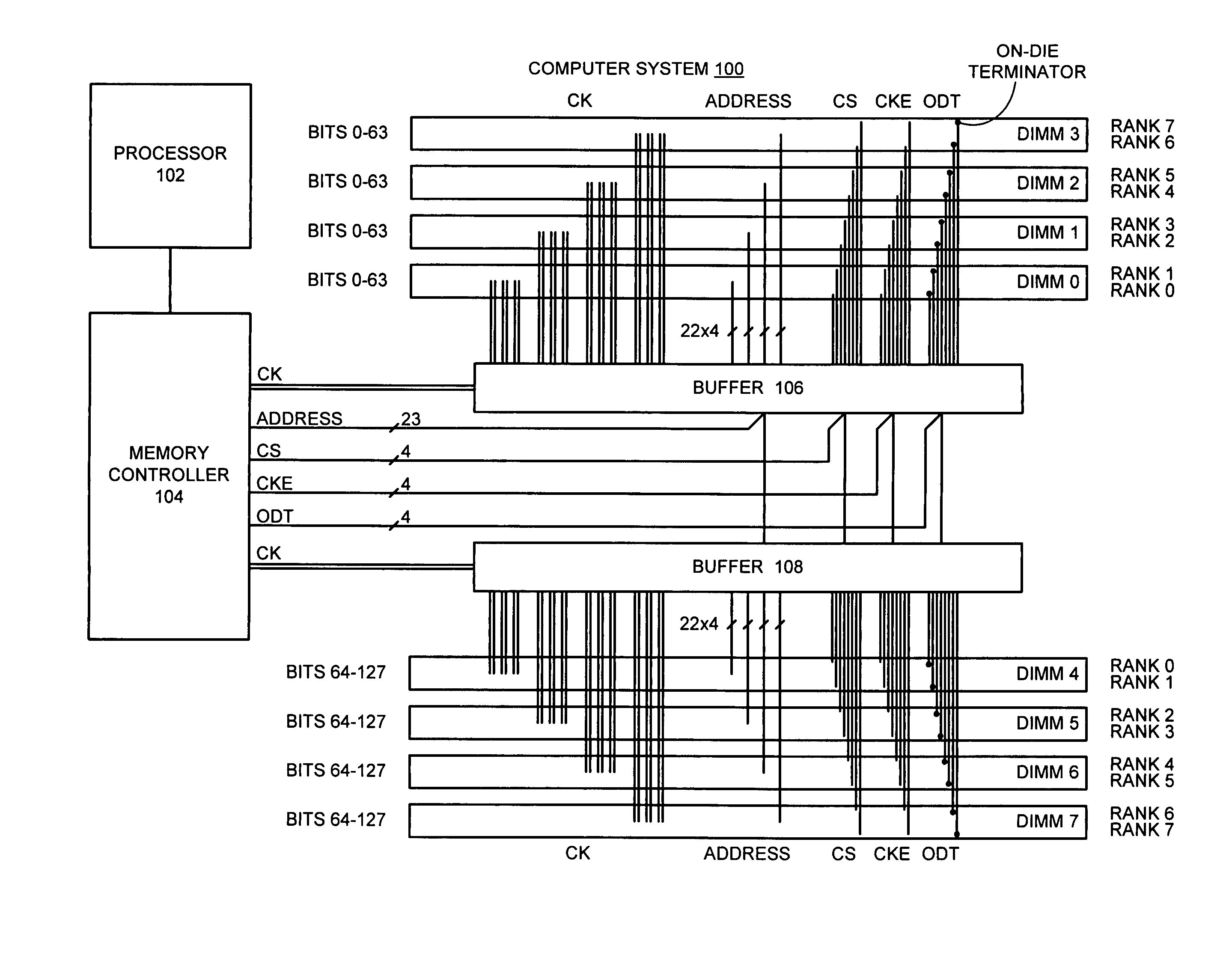
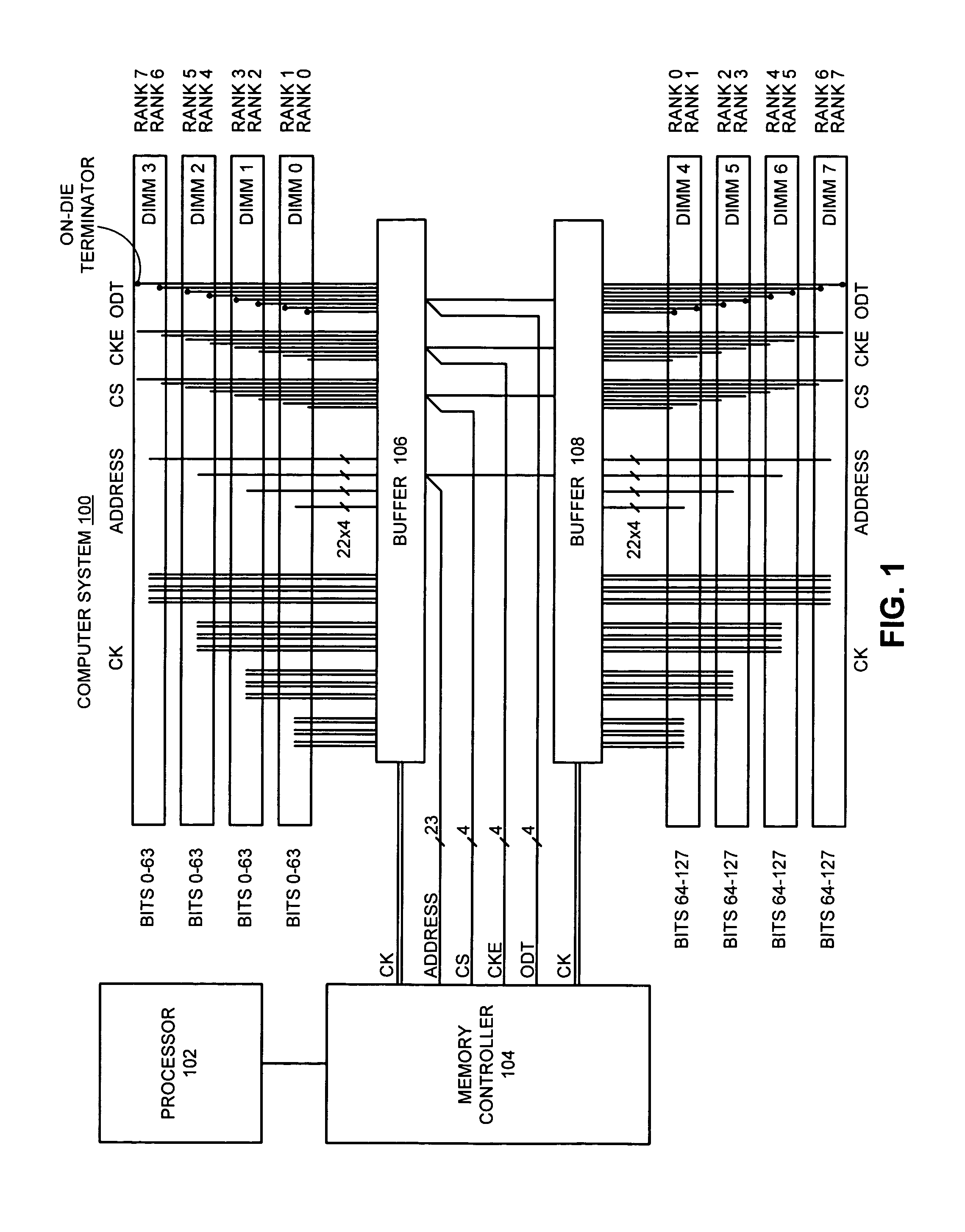
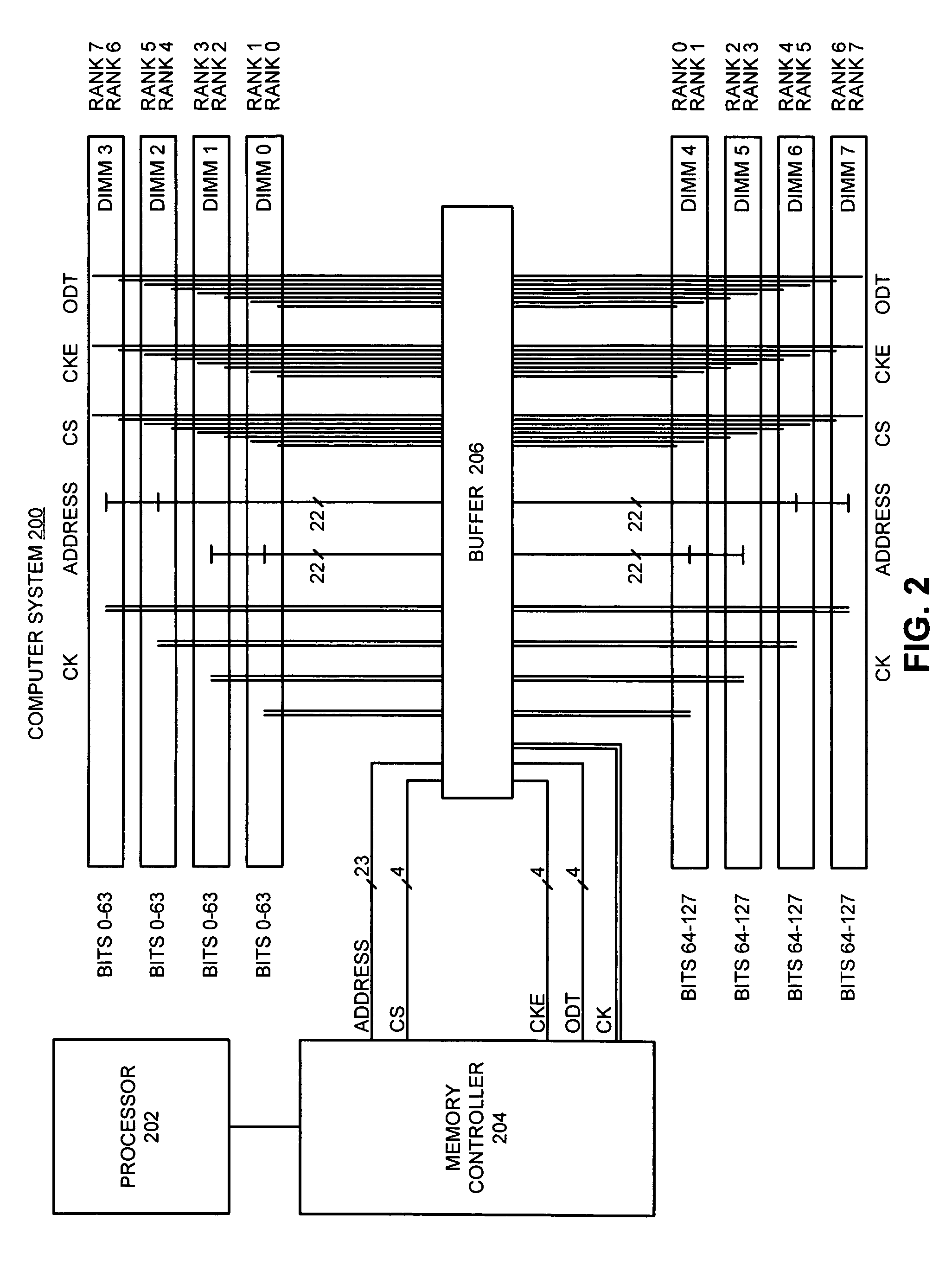
[0036]FIG. 1 illustrates a computer system 100 including two buffer chips 106 and 108 for address and memory control signals in accordance with an embodiment of the present invention. Computer system 100 can generally include any type of computer system, including, but not limited to, a computer system based on a micr...


PUM


Abstract

One embodiment of the present invention provides a system that reduces the number of power and ground pins required to drive address signals to system memory. During operation, the system receives address signals associated with a memory operation from a memory controller, wherein the address signals are received at a buffer chip, which is external the memory controller. The system also receives chip select signals associated with the memory operation at the buffer chip. Next, the system uses the chip select signals to identify an active subset of memory modules in the system memory, which are active during the memory operation. The system then uses address drivers on the buffer chip to drive the address signals only to the active subset of memory modules, and not to other memory modules in the system memory. In this way, the buffer chip requires fewer power and ground pins for the address drivers because the address signals are only driven to the active subset of memory modules, instead of being driven to all memory modules in the system memory.

Description

RELATED APPLICATION[0001]The subject matter of this application is related to the subject matter in a co-pending non-provisional application by the same inventor as the instant application and filed on the same day as the instant application entitled, “Method and Apparatus for Encoding Memory Control Signals to Reduce Pin Count,” having 23 Aug. 2004, and filing date Ser. No. 10 / 925,173.BACKGROUND[0002]1. Field of the Invention[0003]The present invention relates to the design of circuitry within computer systems. More specifically, the present invention relates to a method and an apparatus for reducing the number of pins on semiconductor chips, which are required to communicate address and control signals to memory modules within a computer system.[0004]2. Related Art[0005]As processor clock speeds continue to increase at an exponential rate, larger amounts of data are being transferred at correspondingly faster rates between processor and memory. To accomplish this, computer system ...

Claims


Application Information

Patent Timeline
Patent Type & Authority Patents(United States)
IPC IPC(8): G11C5/14
CPCG06F13/1673G11C5/04G11C7/1045G11C5/066Y02B60/1228Y02D10/00
Inventor CORNELIUS, WILLIAM P.
Owner APPLE INC
Learn More