EMI cancellation method and system

a cancellation method and electromagnetic interference technology, applied in the field of electromagnetic interference cancellation methods and systems, can solve problems such as increasing manufacturing costs and system complexity, affecting the effect of the cancellation method, and affecting the effect of the cancellation

Active Publication Date: 2007-10-30
SEMICON COMPONENTS IND LLC
View PDF5 Cites 23 Cited by
  • Summary
  • Abstract
  • Description
  • Claims
  • Application Information

AI Technical Summary

Benefits of technology

[0009]It is an advantage of the present invention to perform electromagnetic interference cancellation without an additional noise cancellation device.
[0010]To achieve the above object, the electromagnetic interference cancellation system continuously changes the operation frequency of the oscillator.
[0011]In one aspect of the present invention, the electromagnetic interference cancellation system comprises a control signal generation unit, a voltage control unit, and an oscillator. The control signal generation unit includes a counter for counting n bits so as to output a first output signal of n bits with a count value and a second output signal having level that is opposite to the first output signal, the control signal generation unit alternately outputting the first and second output signals as control signals according to a cycle of the counter. The voltage control unit outputs a voltage having a step index level corresponding to the count value of the control signal, and an oscillator for generating a clock signal having a frequency corresponding to the voltage outputted from the voltage control unit, wherein the oscillator generates a clock signal havi

Problems solved by technology

In particular, high frequency electric noise emitted from an electric device via small integrated chips imparts a negative effect to neighboring components, and the equipment may also experience unwanted effects with the noise generated by neighboring devices.
How

Method used


Image

  • EMI cancellation method and system
  • EMI cancellation method and system
  • EMI cancellation method and system

Examples


Embodiment Construction

[0029]In the following detailed description, only the preferred embodiment of the invention have been shown and described, simply by way of illustration of the best mode contemplated by the inventors of carrying out the invention. As will be realized, the invention is capable of modification in various obvious respects, all without departing from the invention. Accordingly, the drawings and description are to be regarded as illustrative in nature, and not restrictive.

[0030]An electromagnetic interference (EMI) cancellation method and system according to the embodiment of the present invention will be described with reference to the accompanying drawings hereinafter.

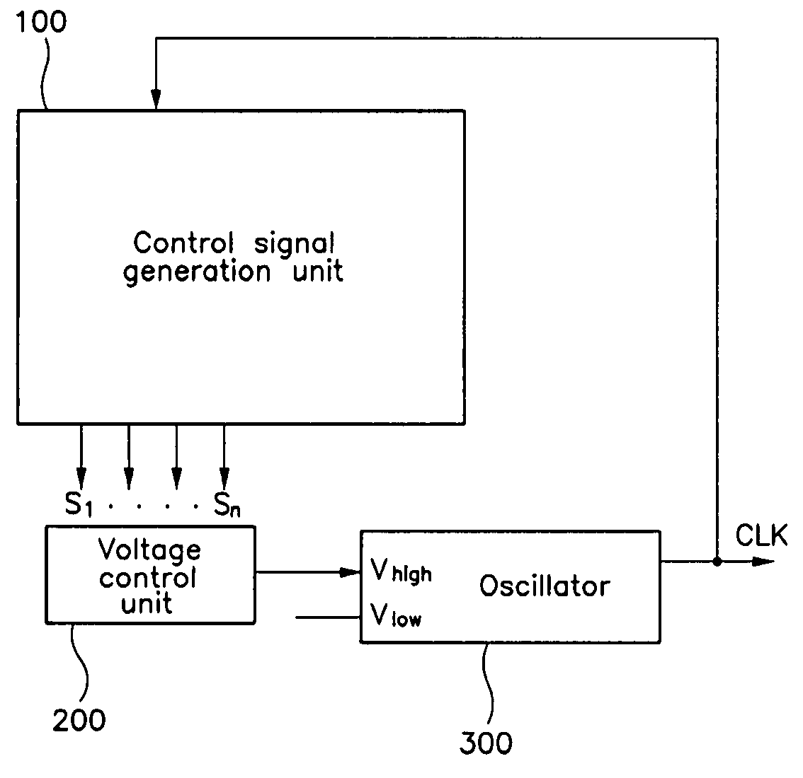
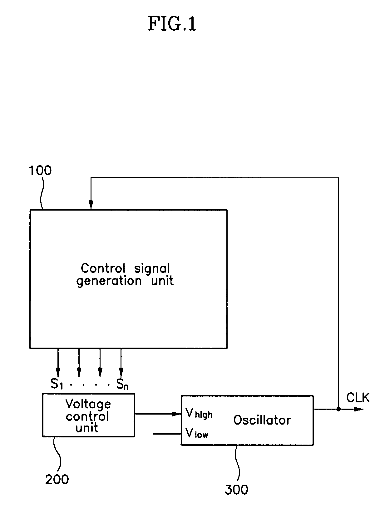
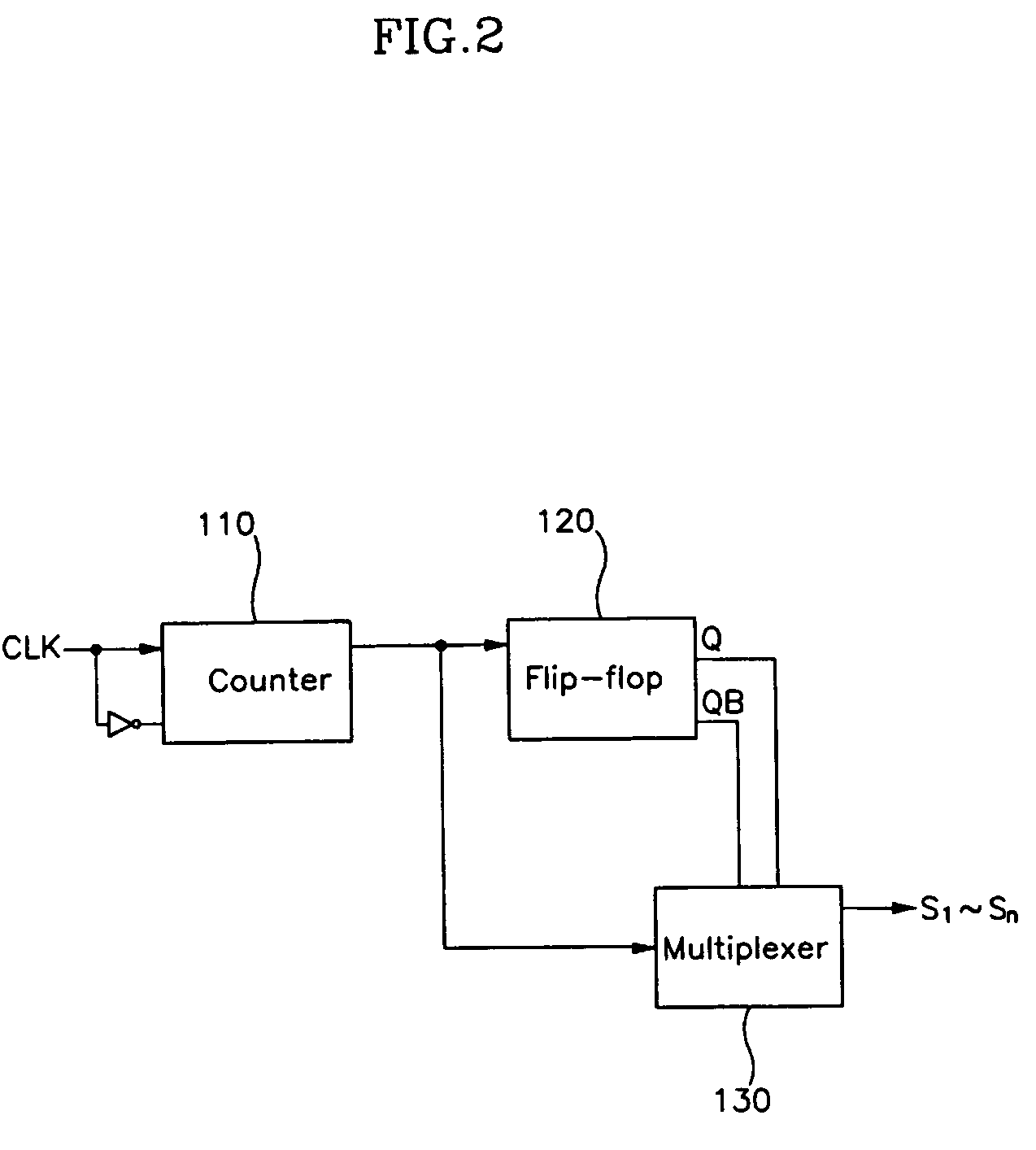
[0031]FIG. 1 is a schematic block diagram illustrating the EMI cancellation system according to the embodiment of the present invention, FIG. 2 is a schematic block diagram illustrating a control signal generation unit of the electromagnetic interference cancellation system according to an embodiment of the present invent...


PUM


Abstract

In an EMI canceller, a control signal generation unit includes a counter, a second flip-flop, and a multiplexer. The counter outputs first and second output signals and includes first flip-flops in series. An output of the first flip-flop reverses at every cycle of the first and second output signals of a previous first flip-flop. An output of the second flip-flop reverses at every cycle of the first or second output signal of a final first flip-flop. The second flip-flop outputs third and fourth output signals. The multiplexer passes the first output signals of the first flip-flop as a control signal when the third output signal is a first level, and passes the second output signals as the control signal when it is a second level.

Description

CROSS REFERENCE TO RELATED APPLICATION[0001]This application is based on Korea Patent Application No. 2002-66134 filed on Oct. 29, 2002 in the Korean Intellectual Property Office, the content of which is incorporated in its entirety herein by this reference.BACKGROUND OF THE INVENTION[0002](a) Field of the Invention[0003]The present invention relates to an electromagnetic interference (EMI) cancellation method and system.[0004](b) Description of the Related Art[0005]The term electromagnetic interference means any electromagnetic disturbance that interrupts, degrades, or limits the effective performance of electrical equipment or systems. In particular, high frequency electric noise emitted from an electric device via small integrated chips imparts a negative effect to neighboring components, and the equipment may also experience unwanted effects with the noise generated by neighboring devices.[0006]The electromagnetic interference intensity depends on the operation speed of semicond...

Claims


Application Information

Patent Timeline
IPC IPC(8): H03D1/04G12B17/02H04B15/02H04L1/00
CPCH04B15/02H04B2215/067G12B17/02
Inventor JANG, KYUNG-OUNKIM, EUNG-SUEN
Owner SEMICON COMPONENTS IND LLC
Why Eureka
Try Eureka