
Method of controlling data transfer within a semiconductor integrated circuit based on a clock sync control signal

a technology of integrated circuits and control signals, applied in the direction of digital transmission, generating/distributing signals, instruments, etc., can solve problems such as attraction of attention, and achieve the effects of reducing power consumption, reducing power consumption, and reducing redundant power consumption in power consumption

Inactive Publication Date: 2007-10-30
SOCIONEXT INC
View PDF21 Cites 2 Cited by
  • Summary
  • Abstract
  • Description
  • Claims
  • Application Information

AI Technical Summary

Benefits of technology

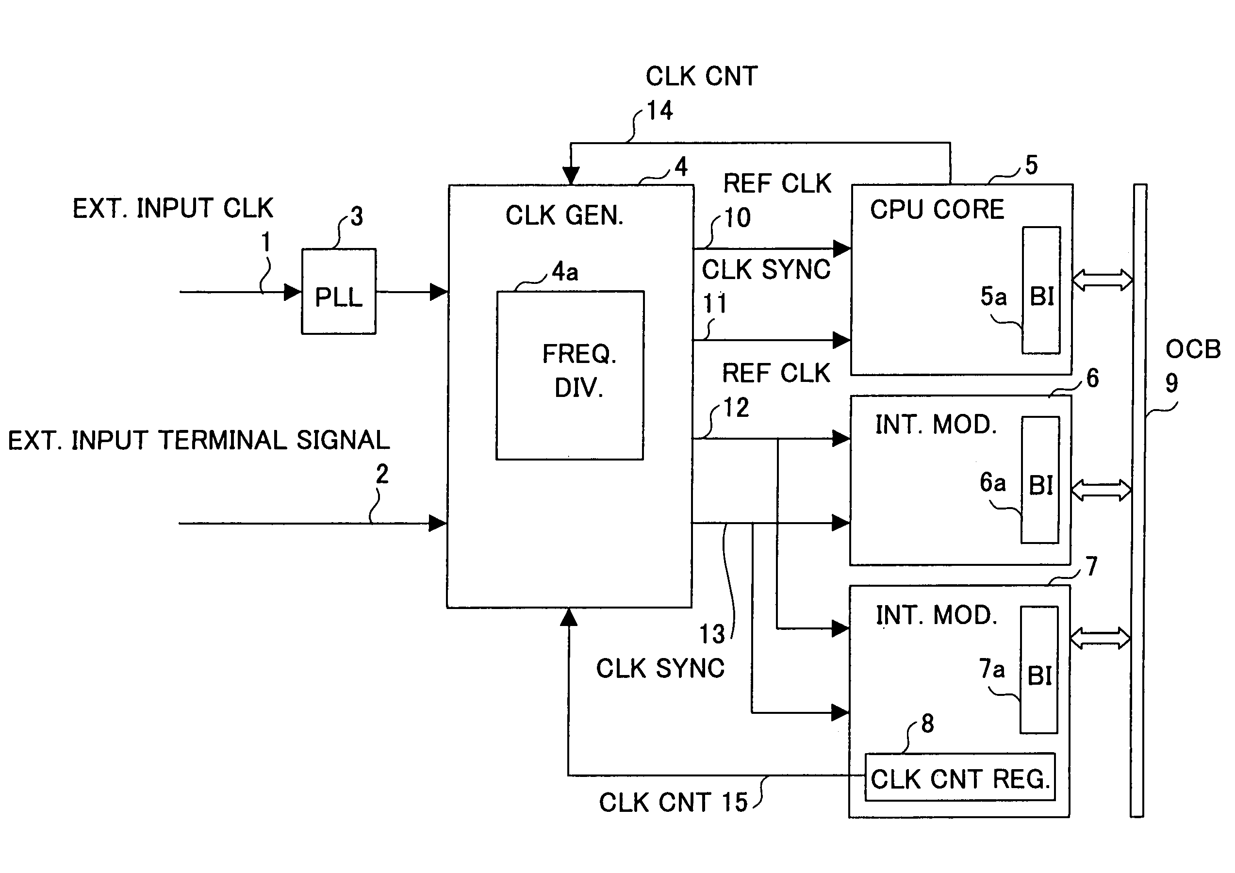
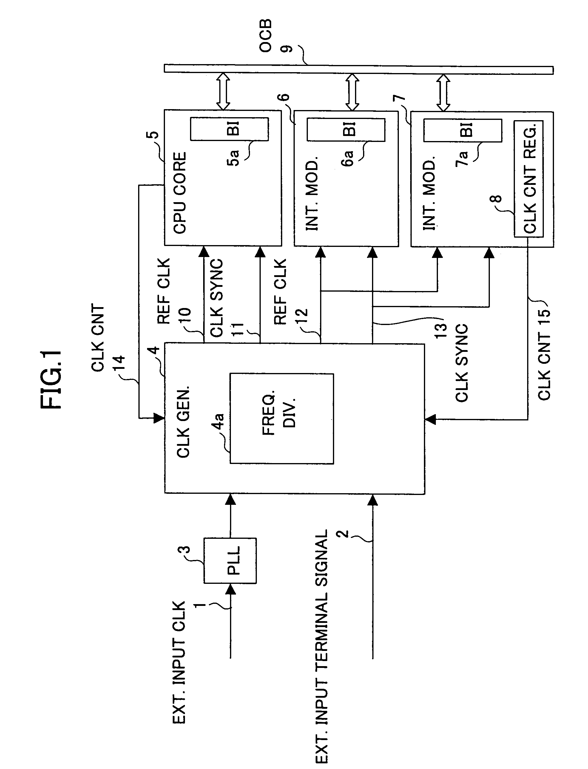
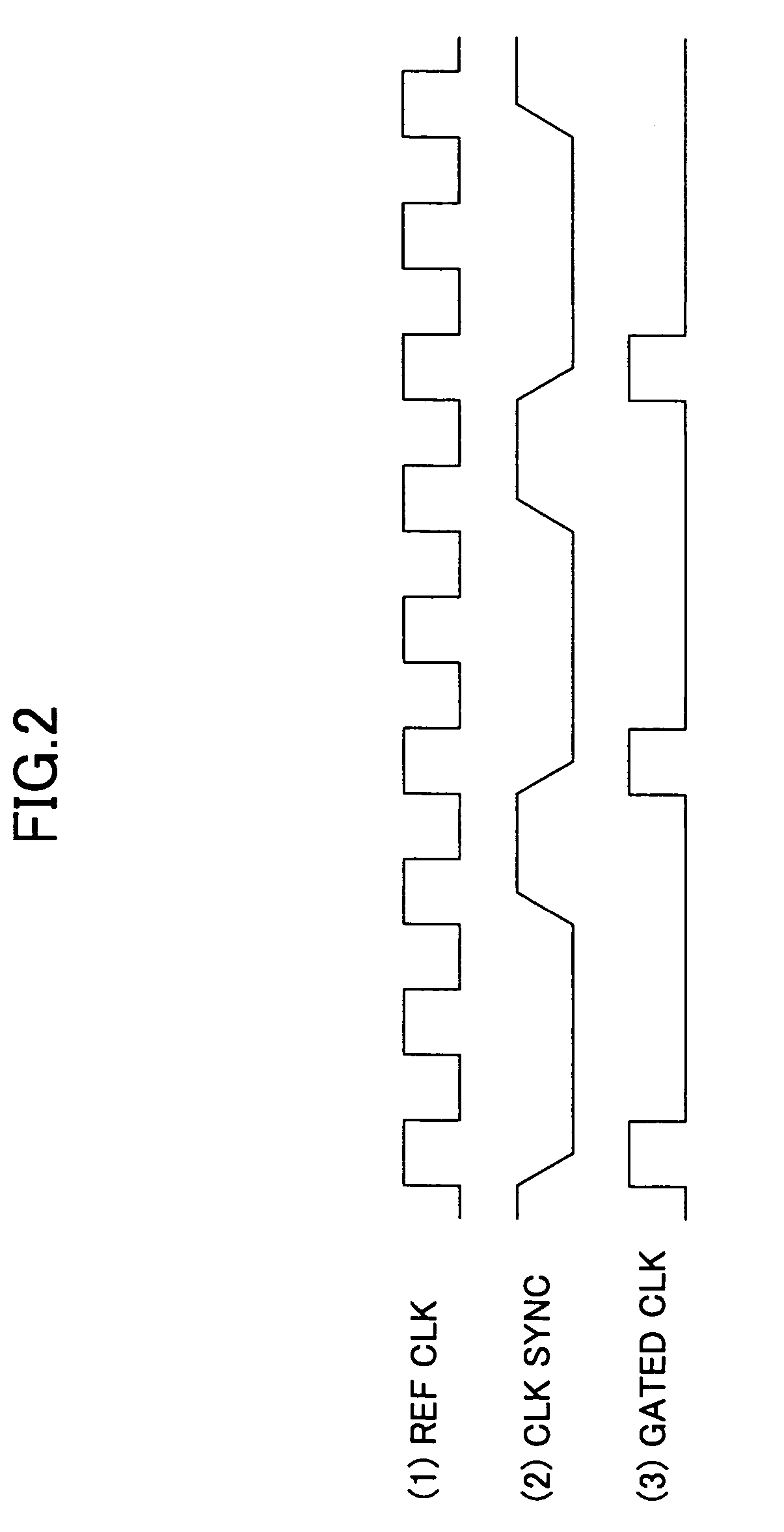
The present invention relates to a semiconductor integrated circuit device comprising an internal bus, multiple internal modules connected to the internal bus, and a clock generating unit. The clock generating unit generates a reference clock and a clock sync signal indicating the positions of valid clock edges. The reference clock and the clock sync signal are supplied to the internal modules for data transfer and processing. The invention reduces redundant power consumption in the clock tree and the modules connected to it, making it effective for reducing power consumption in semiconductor integrated circuit devices with internal modules carrying multiple function IP macro sets. It also allows for operation at the desired operating frequency without carrying out high-speed signal transfer between the modules.

Problems solved by technology

There are many methods of attaining reduction of power consumption by controlling the source power voltage V. In recent years, however, the method of controlling the clock supply to the neighboring modules of which operation is not demanded attracts the attention.

Method used


Image

  • Method of controlling data transfer within a semiconductor integrated circuit based on a clock sync control signal
  • Method of controlling data transfer within a semiconductor integrated circuit based on a clock sync control signal
  • Method of controlling data transfer within a semiconductor integrated circuit based on a clock sync control signal

Examples


Embodiment Construction

[0055]With the recent progress of system LSI development, the development of system-on-chip (SOC) in which a number of function IP macro sets (the functional units for realizing the specific functions) are carried on a single chip is possible. As the circuit scale grows large, the power consumption becomes larger accordingly. Therefore, how the power consumption is reduced is the important subject.

[0056]The system-on-chip (SOC) is usually provided with the internal modules in which many function macro sets are carried. As the measure against the power consumption of the internal modules, the conventional method utilizes the register which indicates whether the operation of each module is activated or not. In the conventional method, when it is detected that a specific module is in inactive state (which indicates the operation thereof is impossible or unnecessary) using the register, the supply of the clock to the module is stopped or turned OFF.

[0057]However, in the conventional met...


PUM


Abstract

A semiconductor integrated circuit device comprises an internal bus, a plurality of internal modules connected to the internal bus and including a main module performing a predetermined function, and a clock generating unit generating a reference clock and a clock sync signal which indicates positions of valid clock edges in the reference clock, the clock generating unit supplying the reference clock and the clock sync signal to the internal modules. At least one of the internal modules is provided with a sync control module which generates an internal clock based on the reference clock and the clock sync signal.

Description

CROSS-REFERENCE TO RELATED APPLICATIONS[0001]This application is based upon and claims the benefit of priority from the prior Japanese patent application No. 2003-204617, filed on Jul. 31, 2003, the entire contents of which are incorporated herein by reference.BACKGROUND OF THE INVENTION[0002]1. Field of The Invention[0003]The present invention relates to a semiconductor integrated circuit device, a clock sync control method and a data transfer control method, which are provided for reducing power consumption of an internal module connected to a bus. More specifically, the present invention relates to a semiconductor integrated circuit device, a clock sync control method and a data transfer control method, which control the operating frequency of the internal module and the internal bus, and attain reduction of power consumption by controlling a clock and a clock sync signal.[0004]2. Description of the Related Art[0005]In recent years, with the development of high-speed, large-scale...

Claims


Application Information

Patent Timeline
Patent Type & Authority Patents(United States)
IPC IPC(8): G06F1/12G06F13/42G06F1/04G06F1/10H04L7/00
CPCG06F1/12G06F1/10
Inventor SHIKATA, TAKASHI
Owner SOCIONEXT INC
Learn More