Optoelectronic fiber photodetector

a technology of optoelectronic fiber and photodetector, which is applied in the direction of optical radiation measurement, instruments, spectrophotometry/monochromator, etc., can solve the problems of microfabrication techniques restricted to planar conformality and planar geometries, and limited device extent and/or material coverage area, and requiring very large capital expenditures

Active Publication Date: 2007-11-06
MASSACHUSETTS INST OF TECH
View PDF27 Cites 38 Cited by
  • Summary
  • Abstract
  • Description
  • Claims
  • Application Information

AI Technical Summary

Problems solved by technology

But in general, microfabrication techniques are restricted to planar geometries and planar conformality and limited device extent and / or materials coverage area.
Microfabricated devices and systems also in general require packaging and typically necessitate very large capital expenditures.

Method used


Image

  • Optoelectronic fiber photodetector
  • Optoelectronic fiber photodetector
  • Optoelectronic fiber photodetector

Examples


examples

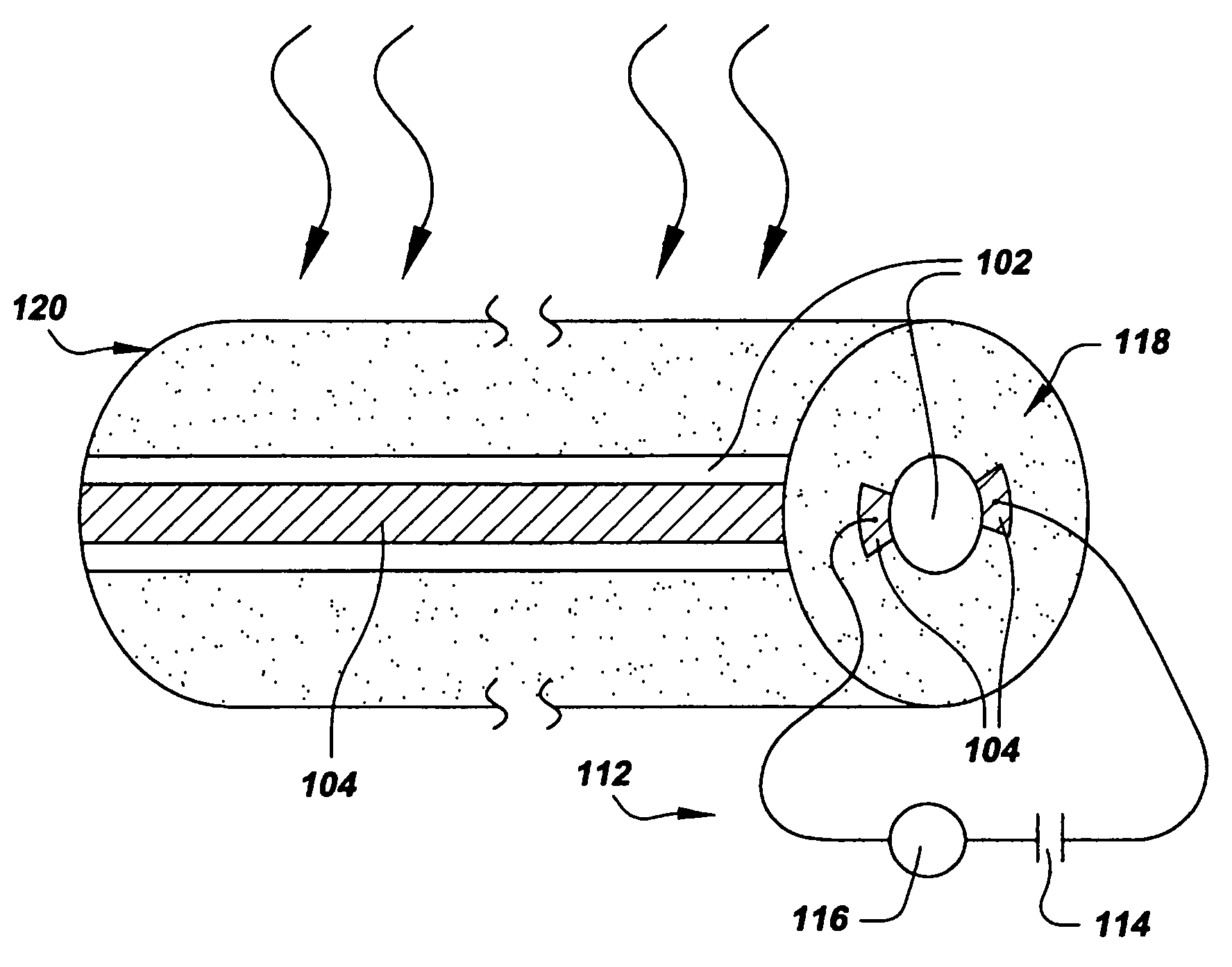
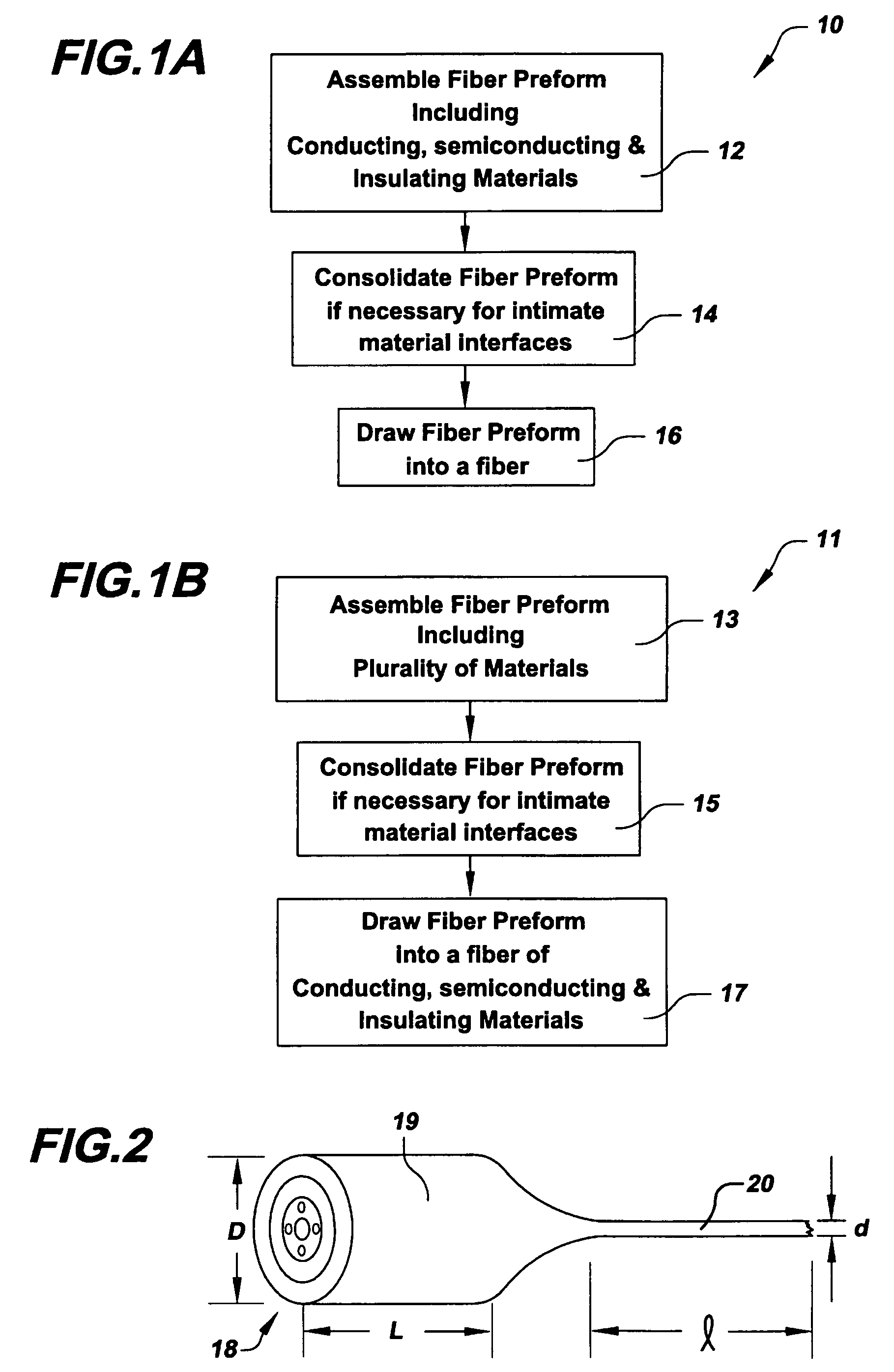
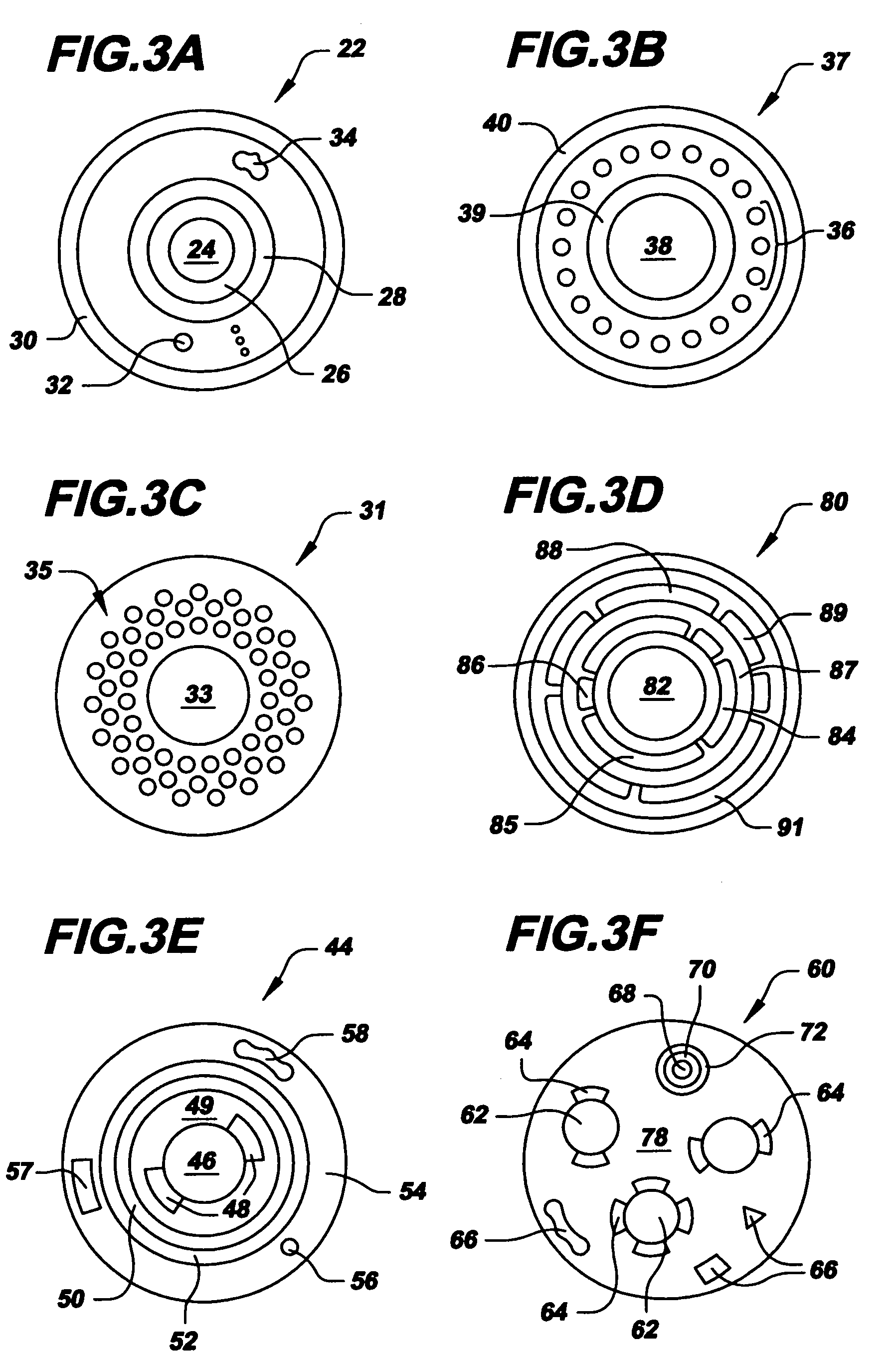
[0127]Referring to FIG. 4, a fiber 90 for conducting both photons and electrons was produced in accordance with the invention. A photon conducting region was provided as a hollow fiber core 92 around which was provided a multilayer photonic bandgap structure 94 of alternating semiconducting and insulating material layers. The bandgap structure exhibited a photonic bandgap at the wavelength corresponding to photon transmission. Sixty cylindrical strands 96 each having an Sn core and polymer cladding were provided around the bandgap structure, and additional polymer reinforcement material 98 was provided around the strands.

[0128]While this example bandgap structure is an omnidirectional reflecting mirror, fibers of the invention are not limited to such; the bandgap structure need not be a multilayer or 1D photonic bandgap structure and instead can exhibit a 2D or 3D photonic bandgap employing structures having periodicities in more than one direction. In the bandgap structure shown, t...


PUM

PropertyMeasurementUnit
operating temperatureaaaaaaaaaa
viscosityaaaaaaaaaa

Abstract

The invention provides an optical fiber photodetector including a photoconductive element, such as a semiconducting element, having a fiber length. The semiconducting element is characterized as a non-composite material in at least one fiber direction. At least one pair of conducting electrodes is in contact with the semiconducting element along the fiber length, and an insulator is provided along the fiber length. An optical resonator can be disposed along the fiber length and along a path of illumination to the semiconducting element. The resonator is dimensioned to substantially reflect all illumination wavelengths except for a prescribed range of wavelengths transmitted to the semiconducting element. The fiber photodetector can be arranged in a photodetecting fiber grid, photodetecting fiber fabric, or other configuration for detecting incident illumination.

Description

[0001]This application claims the benefit of U.S. Provisional Application No. 60 / 584,954, filed Jul. 2, 2004, the entirety of which is hereby incorporated by reference. The application is a continuation in part of copending U.S. application Ser. No. 10 / 890,948 filed Jul. 14, 2004, which in turn claims the benefit of U.S. Provisional Application No. 60 / 487,125, filed Jul. 14, 2003, and U.S. Provisional Application No. 60 / 539,470, filed Jan. 27, 2004, the entirety of both of which are hereby incorporated by reference.STATEMENT REGARDING FEDERALLY SPONSORED RESEARCH[0002]This invention was made with Government support under Contract No. DAAD19-01-0647, awarded by DARPA, under Contract No. ECS-0123460, awarded by the NSF, under Contract No. DMR 02-13282 awarded by the NSF, under contract N00014-02-1-0717 awarded by ONR, under Contract No. Y77011 awarded by AFOSR, and under Contract No. DE-FG02-99ER45778 awarded by DOE. The Government has certain rights in the invention.BACKGROUND OF INV...

Claims


Application Information

Patent Timeline
Patent Type & Authority Patents(United States)
IPC IPC(8): G02B6/26G02B6/02G02B6/036G02B6/44
CPCC03B37/026G01J3/02G01J3/0218H01L27/14601H01L31/035281H01L31/09H01L27/1446G01J2003/1213Y02E10/50
Inventor BAYINDIR, MEHMETSORIN, FABIENABOURADDY, AYMAN F.HINCZEWSKI, DURSEN SAYGINSHAPIRA, OFERARNOLD, JERIMYVIENS, JEAN F.FINK, YOELJOANNOPOULOS, JOHN D.
Owner MASSACHUSETTS INST OF TECH
Why Eureka
Try Eureka