Semiconductor integrated circuit device

a technology of integrated circuits and semiconductors, applied in the direction of instruments, television systems, color signal processing circuits, etc., can solve the problems of difficult to obtain a minute capacity, fixed pattern noise may occur on the screen, etc., and achieve the effect of providing gain uniformity during interleave operation

Active Publication Date: 2007-11-13
RENESAS ELECTRONICS CORP
View PDF8 Cites 30 Cited by
  • Summary
  • Abstract
  • Description
  • Claims
  • Application Information

AI Technical Summary

Benefits of technology

[0008]Since two input capacitors share a variable capacitor device as a feedback capacitor, it is possible to provide gain uniformity during interleave operation.

Problems solved by technology

A fixed pattern noise may occur on the screen.
It is actually difficult to obtain a minute capacity that causes the same change in the two sets.

Method used


Image

  • Semiconductor integrated circuit device
  • Semiconductor integrated circuit device
  • Semiconductor integrated circuit device

Examples


Embodiment Construction

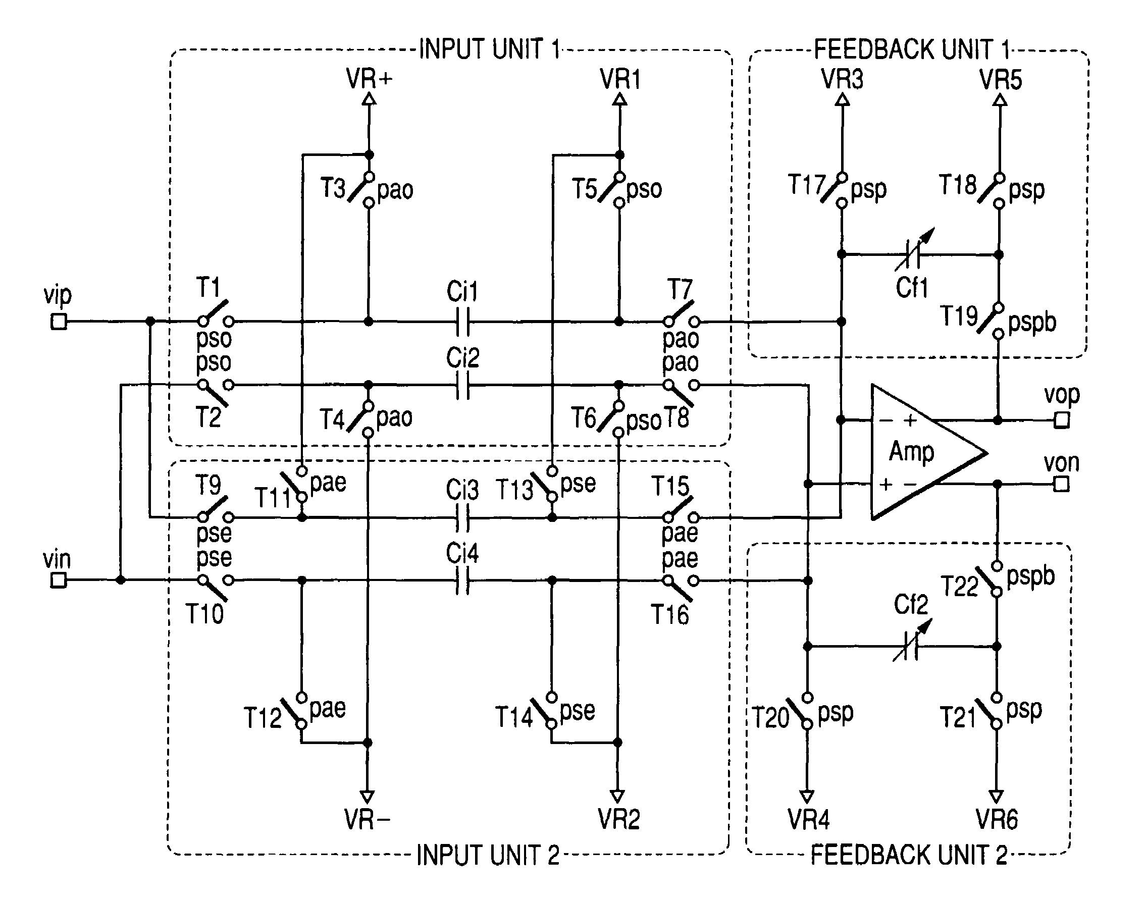
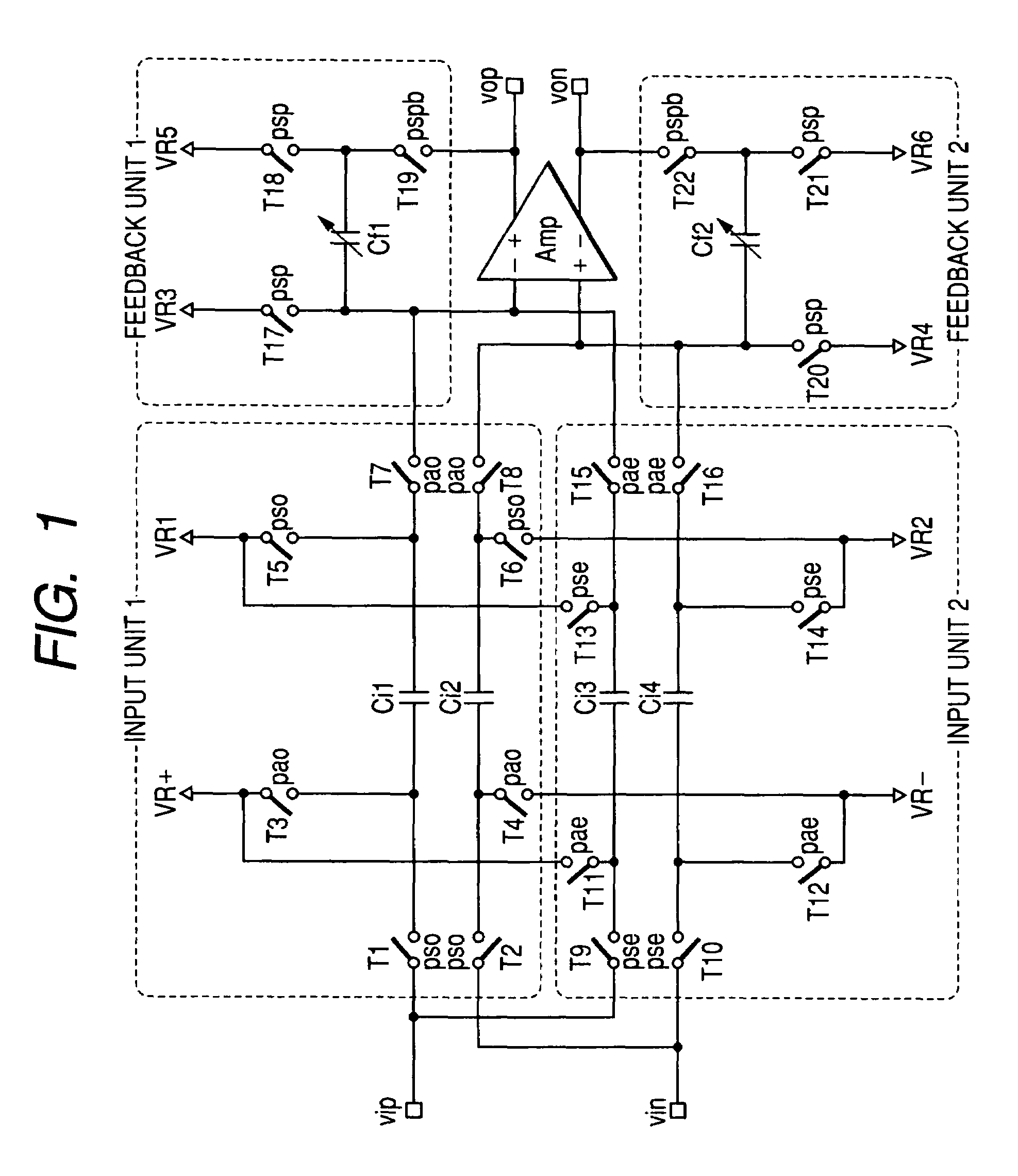
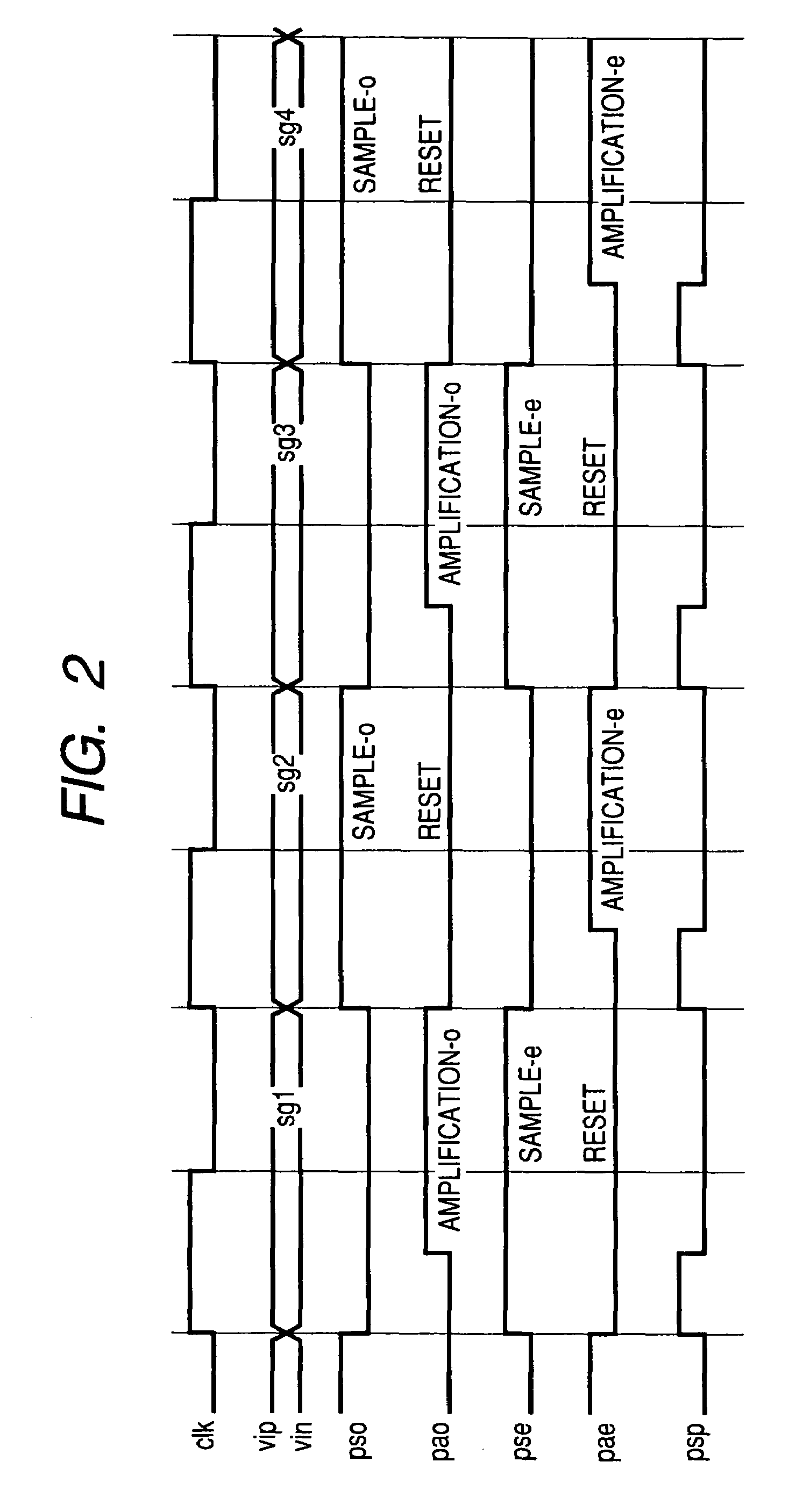
[0021]FIG. 1 provides a circuit diagram showing an embodiment of a variable gain amplifier circuit according to the invention. A known technology to manufacture semiconductor integrated circuits is used to fabricate the variable gain amplifier circuit according to the embodiment. The variable gain amplifier circuit is profitably mounted on a camera preprocessing LSI (AFE, Analog Front End) having variable amplifier circuits such as a correlated double sampling (CDS) circuit and a programmable gain amplifier (PGA).

[0022]The variable gain amplifier circuit according to the embodiment constructs the PGA including: a fully differential amplifier Amp that is mounted on the AFE and has two inputs (positive and negative) and two outputs (positive and negative); and circuit blocks enclosed in dotted lines such as an input unit 1, an input unit 2, a feedback unit 1, and a feedback unit 2. The input 1 is composed of switches T1 through T8 and capacitors Ci1 and Ci2. The input 2 is composed of...


PUM


Abstract

There is a need for providing a variable amplifier circuit suited for a semiconductor integrated circuit and a high-performance camera preprocessing LSI using the variable amplifier circuit. At first timing, a first input capacitor acquires a first signal. An amplifier circuit amplifies a second signal acquired to the second input capacitor according to a gain corresponding to a capacity ratio between the second input capacitor and a feedback capacitor composed of a variable capacitor device. At second timing, the second input capacitor acquires a second signal. The amplifier circuit amplifies the first signal according to a gain corresponding to a capacity ratio between the first input capacitor and the feedback capacitor. A variable gain amplifier circuit interleavingly amplifies the first signal and the second signal in synchronization with the first timing and the second timing.

Description

CROSS-REFERENCE TO RELATED APPLICATION[0001]The present application claims priority from Japanese patent application No. 2005-224795 filed on Aug. 3, 2005, the content of which is hereby incorporated by reference into this application.BACKGROUND OF THE INVENTION[0002]The present invention relates to a semiconductor integrated circuit device, e.g., a technology effectively used for a camera preprocessing LSI (AFE, Analog Front End) having a variable amplifier circuit such as a correlated double sampling (CDS) circuit or a programmable gain amplifier (PGA).[0003]For example, Japanese Unexamined Patent Publication No. 2002-542679 each of the above-mentioned CDS, PGA, and ADC (analog-digital converter) has two sets of input units and common amplifier circuits and performs interleave operation to process signals from an image sensor.[0004][Patent document 1] Japanese Unexamined Patent Publication No. 2002-542679SUMMARY OF THE INVENTION[0005]Patent document 1 above describes that the ampl...

Claims


Application Information

Patent Timeline
Patent Type & Authority Patents(United States)
IPC IPC(8): H03M1/12H04N5/341H04N5/357H04N5/363H04N5/369H04N5/378
CPCH03G1/0094
Inventor AMBO, TAKANOBUIMAIZUMI, EIKIJIMBO, SATOSHI
Owner RENESAS ELECTRONICS CORP
Why Eureka
Try Eureka