
Semiconductor integrated circuit device

a technology of integrated circuit devices and semiconductors, applied in emergency protective circuit arrangements, transistors, etc., can solve the problems of increasing the possibility of reducing the performance of the element, electrostatic discharge, and damage to the semiconductor integrated circuit device, and achieve the effect of small area

Active Publication Date: 2007-11-13
PANNOVA SEMIC
View PDF11 Cites 25 Cited by
  • Summary
  • Abstract
  • Description
  • Claims
  • Application Information

AI Technical Summary

Benefits of technology

"The present invention provides a semiconductor integrated circuit device with an electrostatic discharge protection circuit that is resistant to surges and has a small area. The circuit includes an external connection terminal, an electrostatic discharge protection circuit, a power supply line, a ground line, and an inter-power supply electrostatic discharge protection circuit. The inter-power supply electrostatic discharge protection circuit includes a first NMIS transistor and a first substrate potential control circuit. The substrate potential control circuit can control the substrate potential of the first NMIS transistor to prevent damage to the circuit. The inter-power supply electrostatic discharge protection circuit can discharge a surge through a path that leads from the electrostatic discharge protection circuit to the power supply line and the ground line, resulting in a larger amount of surge current and better resistance to surges. The first NMIS transistor can be turned on more quickly and the potential difference between the substrate potential and the gate potential is reduced, reducing the load on the gate insulating film and preventing destruction of the circuit."

Problems solved by technology

Accordingly, semiconductor integrated circuit devices are vulnerable to damage caused by electrostatic discharge (hereinafter, called “surge”).
For example, a surge penetrated from an external connection terminal might destroy an element such as an input circuit, an output circuit, an input / output circuit or an internal circuit, thus increasing the possibility of reduction in performance of the element.
Hence, the capabilities of these transistors to withstand high voltage are more likely to be degraded, and / or these transistors are more likely to be destroyed.

Method used


Image

  • Semiconductor integrated circuit device
  • Semiconductor integrated circuit device
  • Semiconductor integrated circuit device

Examples


first embodiment

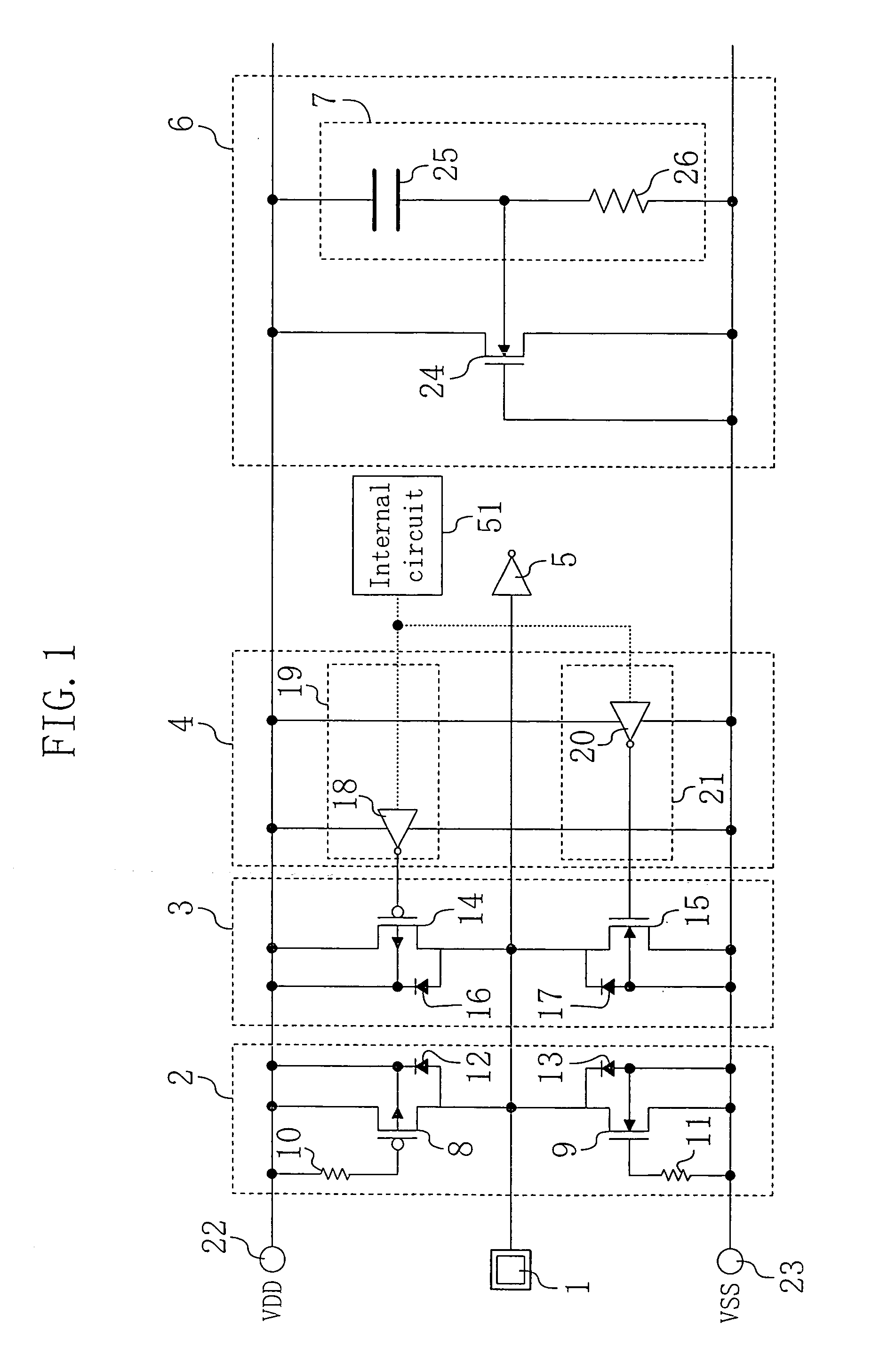
[0073]Hereinafter, a first embodiment of the present invention will be described with reference to the drawings. FIG. 1 is a circuit diagram illustrating the configuration of a semiconductor integrated circuit device including an electrostatic discharge protection circuit according to the first embodiment. Note that FIG. 1 illustrates the configuration of an input / output section of the semiconductor integrated circuit device, and the periphery of the input / output section.

[0074]As shown in FIG. 1, the semiconductor integrated circuit device of this embodiment includes: an external connection terminal 1; an electrostatic discharge protection circuit 2; an output circuit 3; an output prebuffer circuit 4; an input buffer circuit 5; an internal circuit 51; and an inter-power supply electrostatic discharge protection circuit 6. The electrostatic discharge protection circuit 2 and the inter-power supply electrostatic discharge protection circuit 6 are provided in order to protect the outpu...

second embodiment

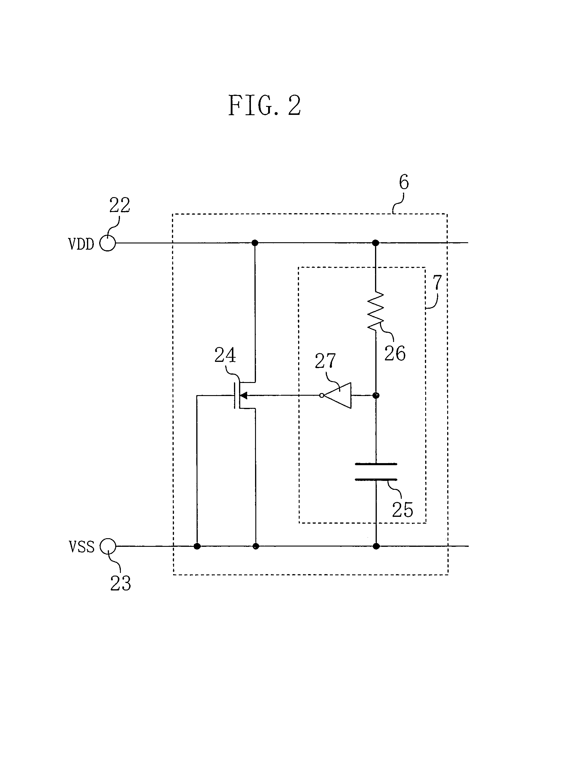
[0087]Hereinafter, a second embodiment of the present invention will be described with reference to the drawings. The semiconductor integrated circuit device of the second embodiment is similar in configuration to that of the first embodiment except for an inter-power supply electrostatic discharge protection circuit, and therefore, description of part of the semiconductor integrated circuit device other than the inter-power supply electrostatic discharge protection circuit will be omitted. FIG. 2 is a circuit diagram illustrating the configuration of the inter-power supply electrostatic discharge protection circuit 6 of the semiconductor integrated circuit device according to the second embodiment.

[0088]As shown in FIG. 2, the inter-power supply electrostatic discharge protection circuit 6 of this embodiment is provided between a power supply line 22 and a ground line 23 and includes an NMIS transistor 24 and a substrate potential control circuit 7. The NMIS transistor 24 includes:...

third embodiment

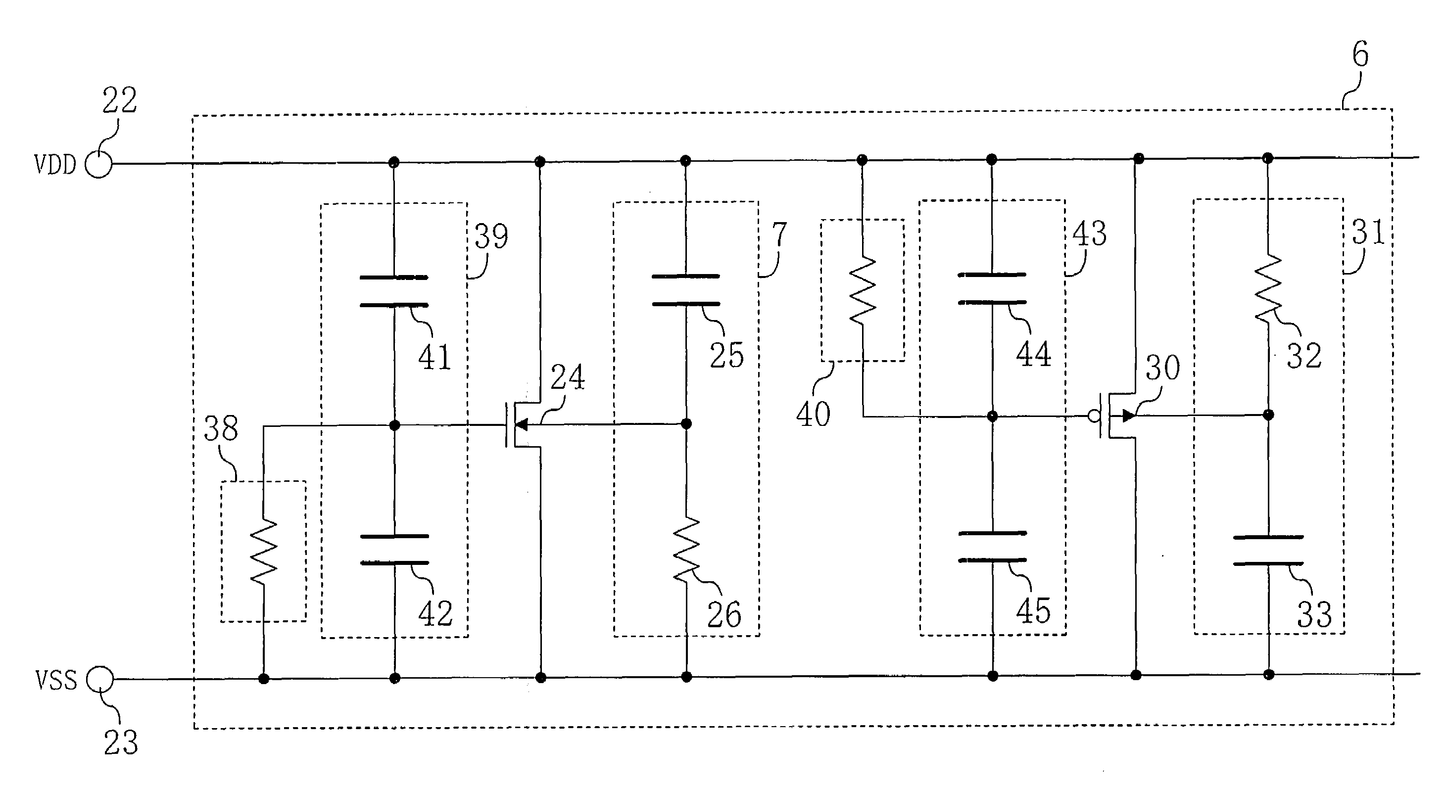
[0097]Hereinafter, a third embodiment of the present invention will be described with reference to the drawings. The semiconductor integrated circuit device of the third embodiment is similar in configuration to that of the first embodiment except for an inter-power supply electrostatic discharge protection circuit, and therefore, description of part of the semiconductor integrated circuit other than the inter-power supply electrostatic discharge protection circuit will be omitted. FIG. 3 is a circuit diagram illustrating the configuration of the inter-power supply electrostatic discharge protection circuit 6 of the semiconductor integrated circuit device according to the third embodiment.

[0098]As shown in FIG. 3, the inter-power supply electrostatic discharge protection circuit 6 of this embodiment is provided between a power supply line 22 and a ground line 23, and includes an NMIS transistor 24 and a substrate potential control circuit 7. The NMIS transistor 24 includes: a source...


PUM


Abstract

An inventive semiconductor integrated circuit device includes: an external connection terminal; an electrostatic discharge protection circuit; an output circuit; an output prebuffer circuit; an input prebuffer circuit; an internal circuit; an inter-power supply electrostatic discharge protection circuit; and a substrate potential control circuit. The substrate potential control circuit includes a capacitor and a resistor. The inter-power supply electrostatic discharge protection circuit includes an NMIS transistor. When a positive surge is applied to the external connection terminal, the substrate potential of the NMIS transistor is also increased. Thus, the NMIS transistor is turned ON, and the positive electrical charge supplied to the external connection terminal is discharged toward a ground line.

Description

CROSS-REFERENCE TO RELATED APPLICATION[0001]This application claims priority under 35 U.S.C. §119(a) on Japanese Patent Application No. 2003-295245 filed on Aug. 19, 2003, the entire contents of which are hereby incorporated by reference.BACKGROUND OF THE INVENTION[0002]The present invention relates to a semiconductor integrated circuit device including an electrostatic discharge (ESD) protection circuit, and more particularly relates to a semiconductor integrated circuit device including an ESD protection circuit having an improved capability for protecting an input circuit, an output circuit, an input / output circuit and an internal circuit from ESD.[0003]In recent years, in the processing of semiconductor integrated circuit devices, the level of integration has been increased in accordance with technical advances in miniaturization and achievement of higher density. Accordingly, semiconductor integrated circuit devices are vulnerable to damage caused by electrostatic discharge (he...

Claims


Application Information

Patent Timeline
Patent Type & Authority Patents(United States)
IPC IPC(8): H02H9/00H01L27/04H01L21/822H01L21/8238H01L23/62H01L27/02H01L27/06H01L27/092
CPCH01L27/0266
Inventor ARAI, KATSUYAKOGAMI, TOSHIHIROYABU, HIROAKI
Owner PANNOVA SEMIC
Learn More