
Semiconductor laser element, method of fabrication thereof, and multi-wavelength monolithic semiconductor laser device

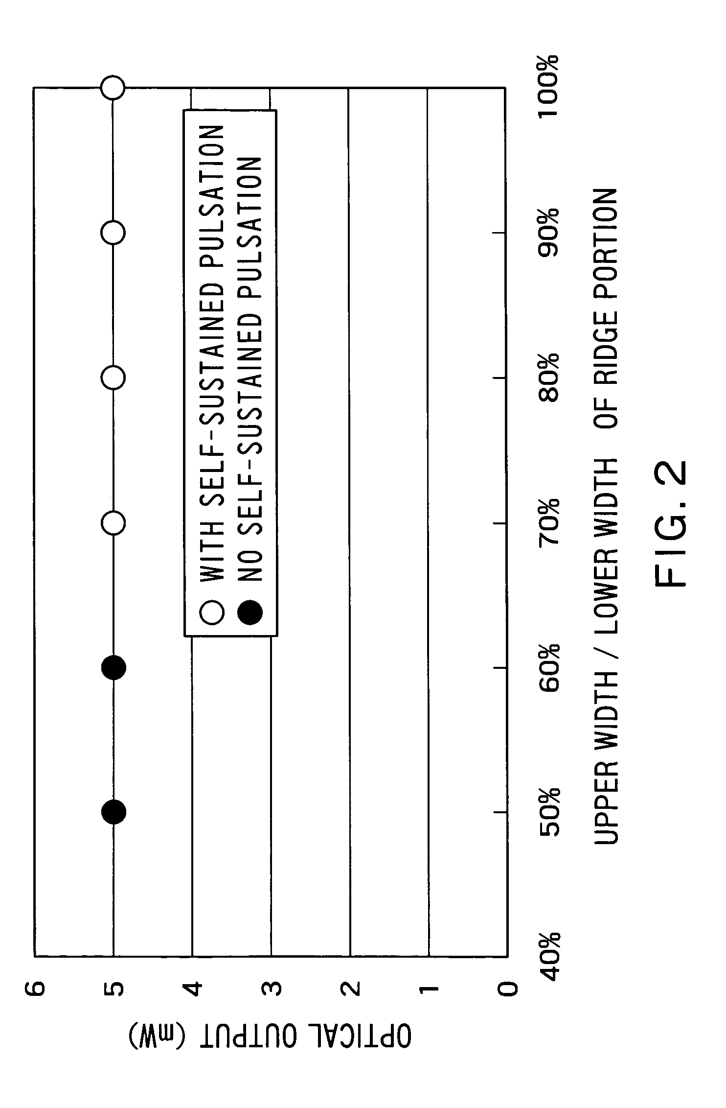
a laser device and semiconductor technology, applied in the direction of lasers, semiconductor laser arrangements, semiconductor lasers, etc., can solve the problem of 4.5 mw as the upper limit of the output region in which self-sustained pulsation is achieved, and achieve the effect of wide output range, high output and increased width of the upper edg

Inactive Publication Date: 2007-11-13
KK TOSHIBA
View PDF7 Cites 3 Cited by
  • Summary
  • Abstract
  • Description
  • Claims
  • Application Information

AI Technical Summary

Benefits of technology

[0016]The present inventors have performed various experiments to obtain a self-sustained pulsation laser which achieves self-sustained pulsation to an output that is higher than that of a self-sustained pulsation laser of the prior art, and which exhibits self-sustained pulsation over a wide output range. As a result, they have overturned conventional technological wisdom and have independently determined that it is possible to obtain self-sustained pulsation up to a high output by shaping each ridge portion so that the width of the upper edge is at least 70% of the width of the lower edge and by increasing the width of the upper edge to greater than that in the prior art.

Problems solved by technology

However, the upper limit of the output region in which self-sustained pulsation is achieved is restricted to approximately 4.5 mW.

Method used


Image

  • Semiconductor laser element, method of fabrication thereof, and multi-wavelength monolithic semiconductor laser device
  • Semiconductor laser element, method of fabrication thereof, and multi-wavelength monolithic semiconductor laser device
  • Semiconductor laser element, method of fabrication thereof, and multi-wavelength monolithic semiconductor laser device

Examples


first embodiment

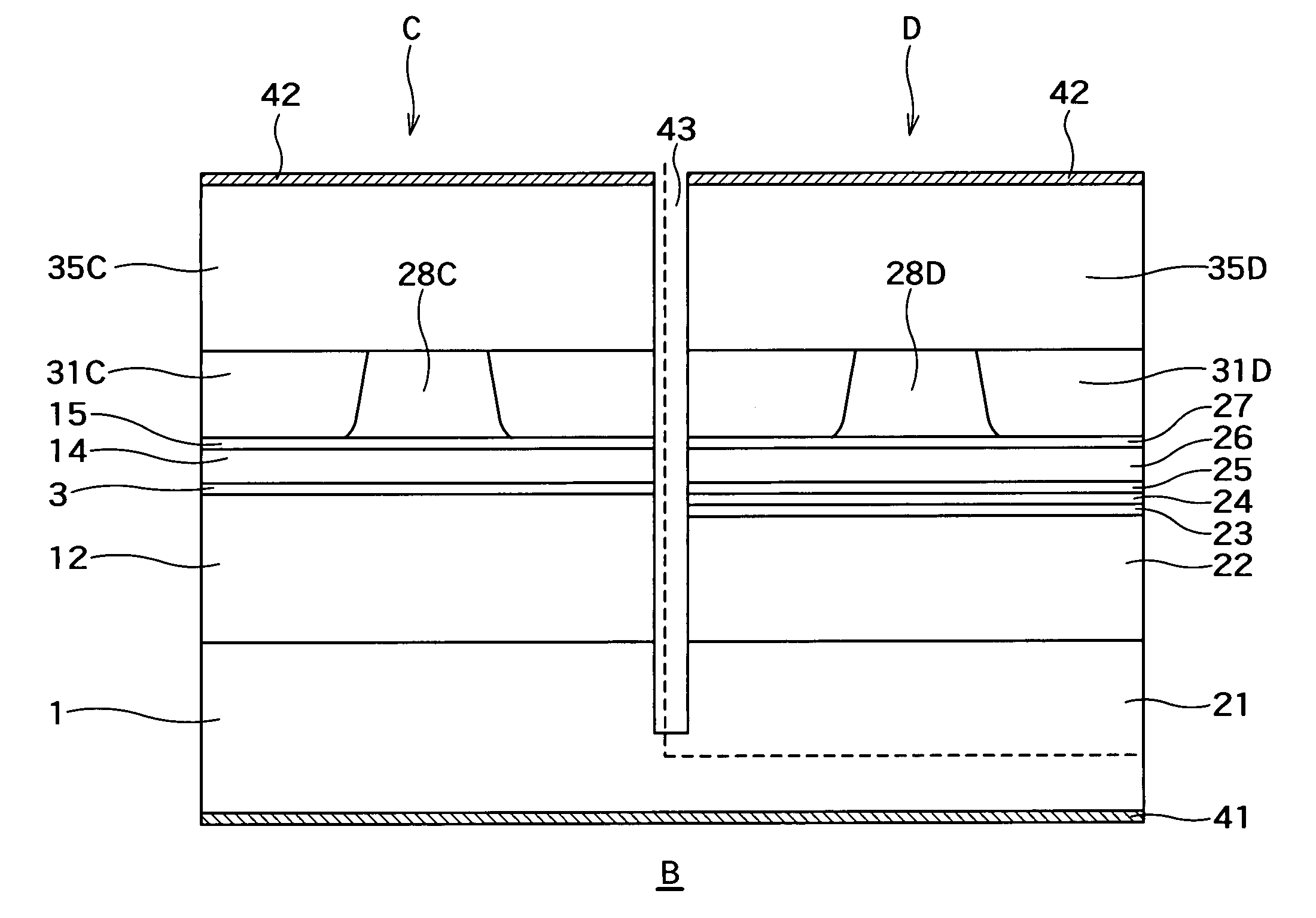
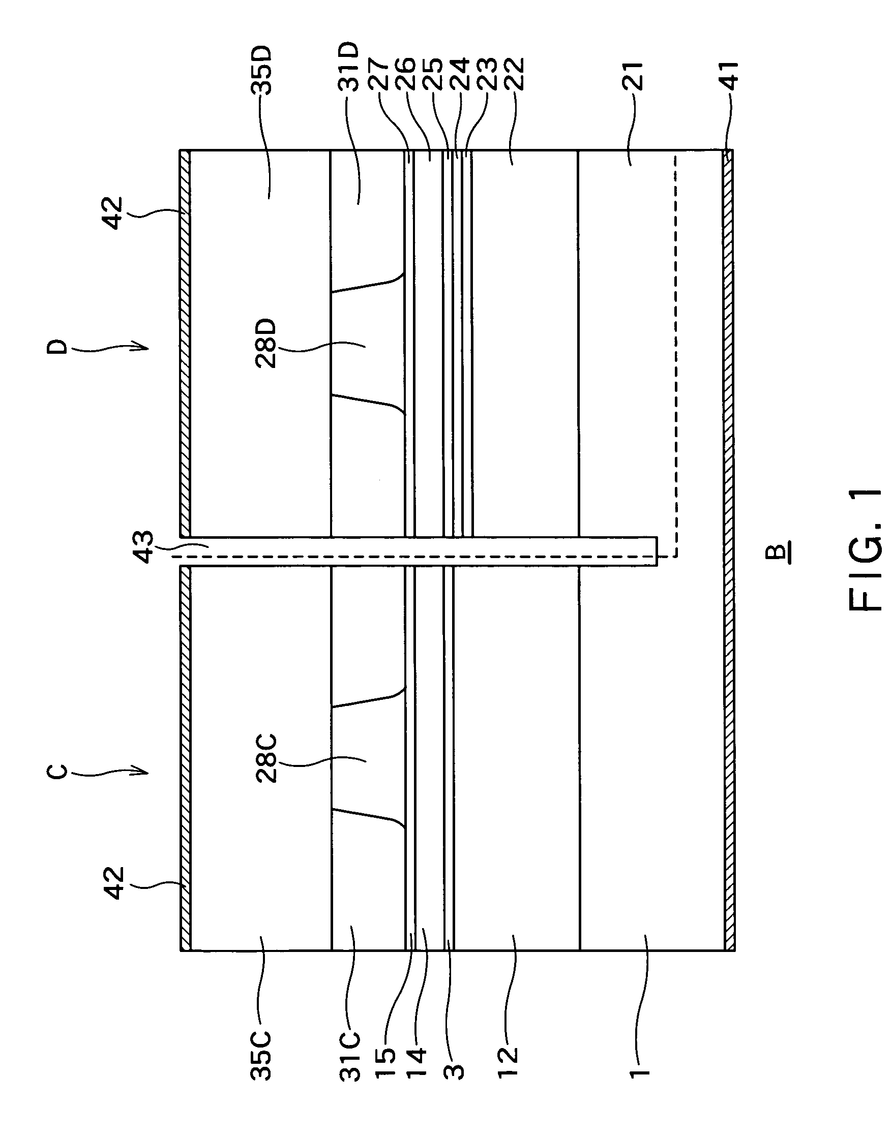
[0054]A section through a two-wavelength monolithic semiconductor laser device B in accordance with a first embodiment of this invention is shown in FIG. 1. This two-wavelength monolithic semiconductor laser device B is provided with an AlGaAs compound semiconductor laser element C in which an active layer 3 is formed of an AlGaAs compound material, on the left side of the figure, and an InGaAlP compound semiconductor laser element D in which an active layer 24 is formed of an InGaAlP compound material, on the right side of the figure. The AlGaAs compound semiconductor laser element C on the left side of the figure is for CDs and the InGaAlP compound semiconductor laser element D on the right side of the figure is for DVDs. The element C of CDs is a laser element of the 780 nm-band and the element D for DVDs is a laser element of the 650-nm band. Note that a laser element of the 780-nm band is an element that emits a laser beam of a wavelength of approximately 770 nm to 790 nm, and ...

second embodiment

[0090]A section through a two-wavelength monolithic semiconductor laser device B in accordance with a second embodiment of the present invention is shown in FIG. 4. This device differs from the device of the first embodiment (shown in FIG. 1) in that dielectric isolation films 29C and 29D of SiO2 are formed to sandwich both sides of the corresponding ridge portions 28C and 28D and the GaAs contact layers 35C and 35D are formed in stripe shapes on the corresponding ridge portions 28C and 28D. The material properties of the dielectric isolation films 29C and 29D and the GaAs contact layers 35C and 35D are the same for the elements C and D on the left and right.

[0091]Since the dielectric isolation films 29C and 29D of SiO2 have a refractive index that is lower than that of InAlP, and thus it is difficult to broaden the guide mode, it is possible to broaden the guide mode and induce self-sustained pulsation by controlling the thicknesses of the p-type first clad layers 14 and 26.

third embodiment

[0092]A perspective view of a two-wavelength monolithic semiconductor laser device B in accordance with a third embodiment of the present invention is shown in FIG. 5. This device differs from the device of the second embodiment (shown in FIG. 4) in that the stripe-shaped second conductive type second semiconductor layers 28C and 28D and the GaAs contact layers are formed to be wider at a central portion between an end surface E at the nearer end and an end surface F at a farther end, and narrower in the vicinity of the end surfaces. It is possible to narrow the guide mode in the lateral direction in the vicinity of the end surfaces and increase the angle of emission of the thus-emitted laser beam in the lateral direction by widening the central portions of the stripe-shaped second conductive type second semiconductor layers 28C and 28D, as shown in FIG. 5. Note that if the width of the stripe-shaped second conductive type second semiconductor layers 28C and 28D in the vicinity of t...


PUM


Abstract

The present invention provides a semiconductor laser element, a method of fabrication thereof, and a multi-wavelength monolithic semiconductor laser device that achieve self-sustained pulsation up to a high output level and achieve self-sustained pulsation over a wide output range. A semiconductor laser element that exhibits self-sustained pulsation in a predetermined output region, said semiconductor laser element comprising: a substrate; a first conductive type clad layer formed on said substrate; an active layer formed on said first conductive type clad layer for emitting light by current injection; a second conductive type first clad layer formed on said active layer; and a stripe-shaped second conductive type second clad layer formed on said second conductive type first clad layer in a first direction, in such a manner that the cross-sectional surface of said stripe-shaped second conductive type second clad layer in a direction perpendicular to said first direction has a shape having an upper edge and a lower edge that face each other and side edges that connect between said upper edge and said lower edge, where the minimum width thereof is at least 70% but no more than 100% of the maximum width.

Description

CROSS-REFERENCE TO RELATED APPLICATIONS[0001]This application is based upon and claims the benefits of priority from the prior Japanese Patent Application No. 2002-349033, filed on Nov. 29, 2002, the entire contents of which are incorporated herein by reference.BACKGROUND OF THE INVENTION[0002]1. Field of the Invention[0003]The present invention relates to a semiconductor laser element, a method of fabrication thereof, and a multi-wavelength monolithic semiconductor laser device.[0004]2. Related Background Art[0005]It is becoming popular to develop an integrated optical unit assembled from a semiconductor laser of a wavelength in the 650-nm band for digital versatile disks (DVDs) and another semiconductor laser of a wavelength in the 780-nm band for CD-ROMs. The development is also proceeding of a two-wavelength monolithic semiconductor laser device in which these two lasers are formed monolithically on the same substrate. To ensure that this two-wavelength monolithic semiconductor ...

Claims


Application Information

Patent Timeline
Patent Type & Authority Patents(United States)
IPC IPC(8): H01S5/00H01S5/22H01S5/065H01S5/223H01S5/323H01S5/343H01S5/40
CPCB82Y20/00H01S5/4031H01S5/2231H01S5/0658H01S5/2206H01S5/4087H01S5/34326H01S5/3436
Inventor TANAKA, AKIRASHIOZAWA, HIDEOWATANABE, MINORUGEN-EI, KOICHITANAKA, HIROKAZU
Owner KK TOSHIBA
Learn More