Methods for producing thin films on substrates by plasma CVD

a technology of plasma cvd and substrate, which is applied in the field of method and system for forming thin films, can solve the problems of difficult formation of thin films, deterioration of film quality, and difficulty in thin film formation, so as to achieve excellent quality, improve film quality, and improve the effect of quality

Inactive Publication Date: 2007-12-04
NGK INSULATORS LTD
View PDF19 Cites 34 Cited by
  • Summary
  • Abstract
  • Description
  • Claims
  • Application Information

AI Technical Summary

Benefits of technology

[0010]The technique described in Japanese patent publication 2002-339, 072A is superior in that a thin film having excellent quality can be formed without inserting an electrode into the inner space in the tubular member. The inventors have studied the technique further, and found that the plasma reaction gas cannot be passed through the space in the tubular member easily as the inner diameter of the tubular member is smaller. The amount of supply of the rea...

Problems solved by technology

The amount of supply of the reaction gas into the space becomes thus smaller, so that the formation of the thin film is made difficult and the quality of the film may be deteri...

Method used


Image

  • Methods for producing thin films on substrates by plasma CVD
  • Methods for producing thin films on substrates by plasma CVD
  • Methods for producing thin films on substrates by plasma CVD

Examples


examples

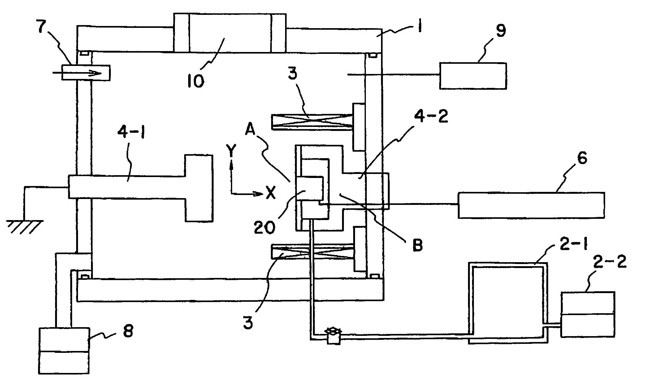
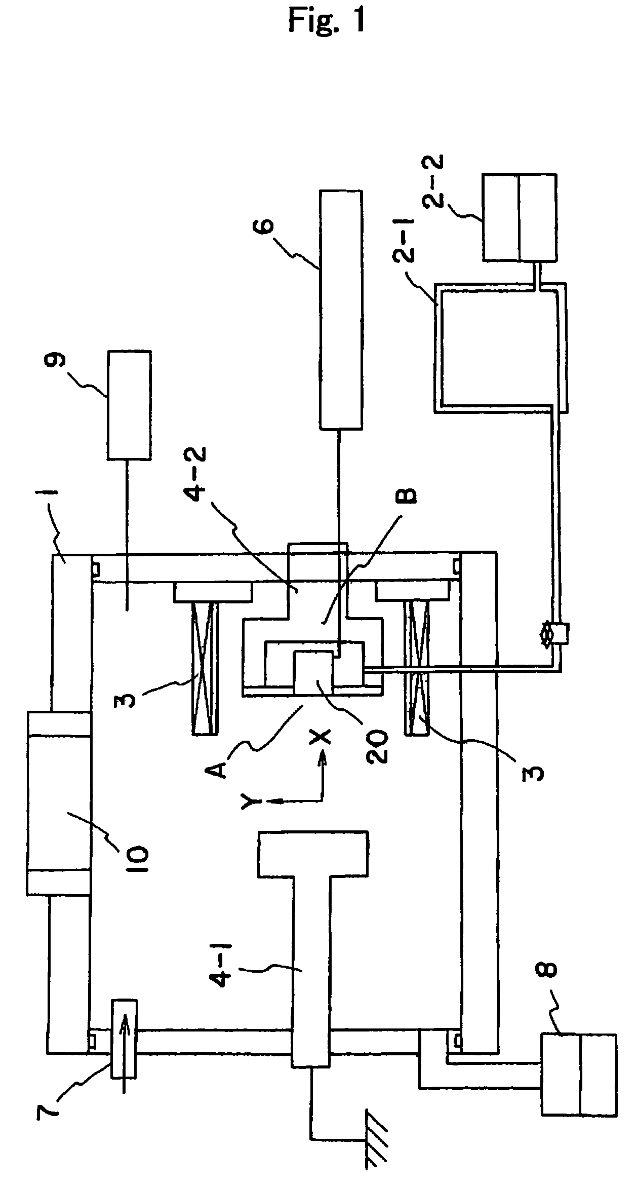
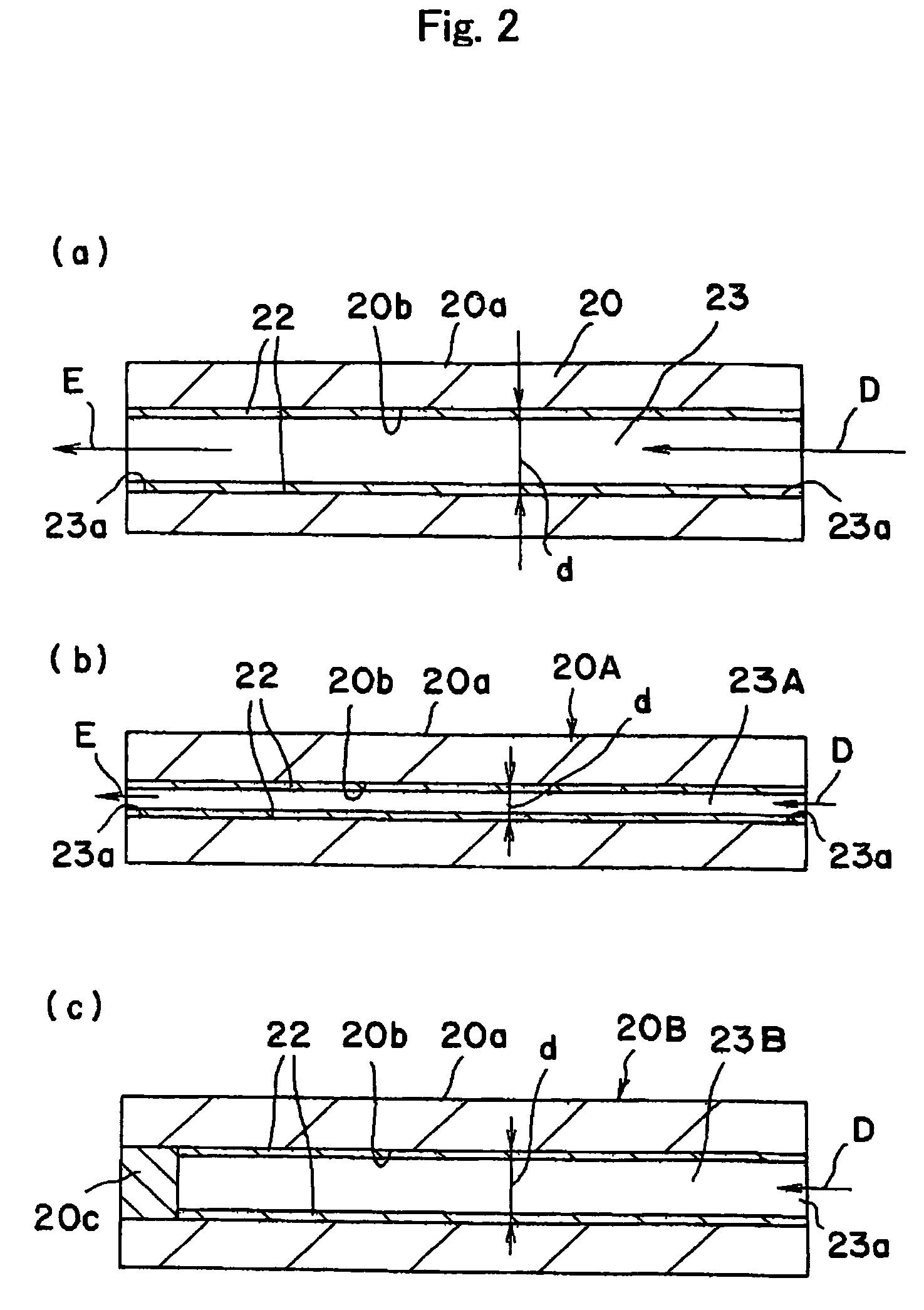
[0043]A film 22 of diamond like carbon was formed on the inner wall surface 20b of the substrate 20B as shown in FIG. 2(c), according to the process described above referring to FIG. 1. Specifically, the outer diameter of the substrate 20B was 5 mm, the inner diameter was 0.9 mm, and the length was 20 mm.

[0044]The substrate 20B was mounted and fixed on the cathode 4-2, and the inside of the chamber 1 was evacuated to a degree of vacuum of 1×10⁻⁴ to 1×10⁻⁵ Torr by means of the pump 8. C2H2 gas was introduced at a flow rate of 20 cm3 / min through the gas supply hole 7, and the pressure in the chamber 1 was maintained at 3.75×10⁻² Torr by controlling the evacuation with the pump 8. 8.0 kV of the pulse voltage was applied between the anode 4-1 and cathode 4-2 with the high voltage pulse source 6 to generate C2H2 gas plasma. A distance between the anode 4-1 and cathode 4-2 was 10 cm, so that an electric field of 80 kV / m was generated between the anode 4-1 and cathode 4-2. The pulse width ...


PUM

PropertyMeasurementUnit
Timeaaaaaaaaaa
Lengthaaaaaaaaaa
Frequencyaaaaaaaaaa

Abstract

Methods are provided to form a thin film reproducibly in a process for forming the thin film on the inner wall surface facing a space formed in a substrate by plasma CVD. A thin film is produced on an inner wall surface of a substrate facing a space formed in the substrate. The substrate is contained in a chamber for plasma CVD process. A gas for plasma reaction is then flown into the space and a pulse voltage is applied on the substrate without substantially applying a direct bias voltage on the substrate to form the thin film on the inner wall surface.

Description

[0001]This application is a non-provisional application of U.S. provisional application 60 / 457,310 filed on Mar. 26, 2003, and Japanese patent application 2003-38,767, filed on Feb. 17, 2003, the entireties of which are incorporated by reference.BACKGROUND OF THE INVENTION[0002]1. Field of the Invention[0003]The present invention provides a method and system for forming a thin film on an inner wall surface of a substrate facing a space formed in the substrate by means of plasma CVD.[0004]2. Related Art Statement[0005]It has been known to form a hard film such as a diamond film or diamond like carbon film on a substrate to impart corrosion resistance to the substrate. Recently, it has been tried to form a hard film on an inner wall surface of a tubular body, whose applications include various products.[0006]Such hard film is formed by so called plasma CVD process. According to the process, for example, a gaseous raw material such as methane gas is introduced with a carrier gas such a...

Claims


Application Information

Patent Timeline
IPC IPC(8): H05H1/24C23C16/04C23C16/515
CPCC23C16/515C23C16/045
Inventor SAITO, TAKAONAKAMURA, YUKINORIKONDO, YOSHIMASAOHTAKE, NAOTO
Owner NGK INSULATORS LTD
Why Eureka
Try Eureka