Compact ternary and binary CAM bitcell architecture with no enclosed diffusion areas

a bitcell and cam bitcell technology, applied in the field of data processing, can solve the problems of significant impact on the performance and/or yield of the memory cell, difficult to set the threshold voltage vt of these devices separately, and relatively difficult to implement polysilicon and contact/metal b>1/b> patterns, so as to avoid unintended variations in electrical performance

Inactive Publication Date: 2007-12-04
AVAGO TECH WIRELESS IP SINGAPORE PTE
View PDF11 Cites 18 Cited by
  • Summary
  • Abstract
  • Description
  • Claims
  • Application Information

AI Technical Summary

Benefits of technology

[0027]The present invention provides layouts of binary and ternary content addressable memory cells. A content addressable memory cell layout according to the invention contains no isolation regions that are surrounded by diffusion regions. Rather, the diffusion regions are designed such that shallow trench isolation stress can exert only minimal influence on the drive current of the memories. The content addressable memory cell layout according to the invention further has transistors that are all oriented in the same direction to avoid unintended variations in electrical performance and can have multiple threshold voltages set for n-type transistors within the same cell. Content addressable memory cell layouts according to the invention are “process friendly” to accommodate requirements of advanced process technologies such as the 90 nm process.

Problems solved by technology

The structure of an isolation region completely surrounded by a diffusion region leads to stress-related effects that can significantly impact the performance and / or yield of the memory cell.
Because of this, it is difficult to set the threshold voltages Vt of these devices separately to optimize their different uses.c) The patterns for polysilicon and for contact / metal 1 are relatively difficult to implement while still achieving a compact cell size.
Because the width of the polysilicon lines in FIG. 4A vary along the length of the line, this design is inherently less conducive to achieving the SPICE modeling targets.
The use of p-channel transistors as access transistors greatly reduces the performance of the SRAM cell (for a given size of transistor used) because PMOS devices inherently have lower channel mobility than NMOS devices.

Method used


Image

  • Compact ternary and binary CAM bitcell architecture with no enclosed diffusion areas
  • Compact ternary and binary CAM bitcell architecture with no enclosed diffusion areas
  • Compact ternary and binary CAM bitcell architecture with no enclosed diffusion areas

Examples


Embodiment Construction

[0040]The invention will now be discussed with regard to several specific embodiments, shown in FIGS. 6A, B and 7A, B.

[0041]Binary CAM Layout

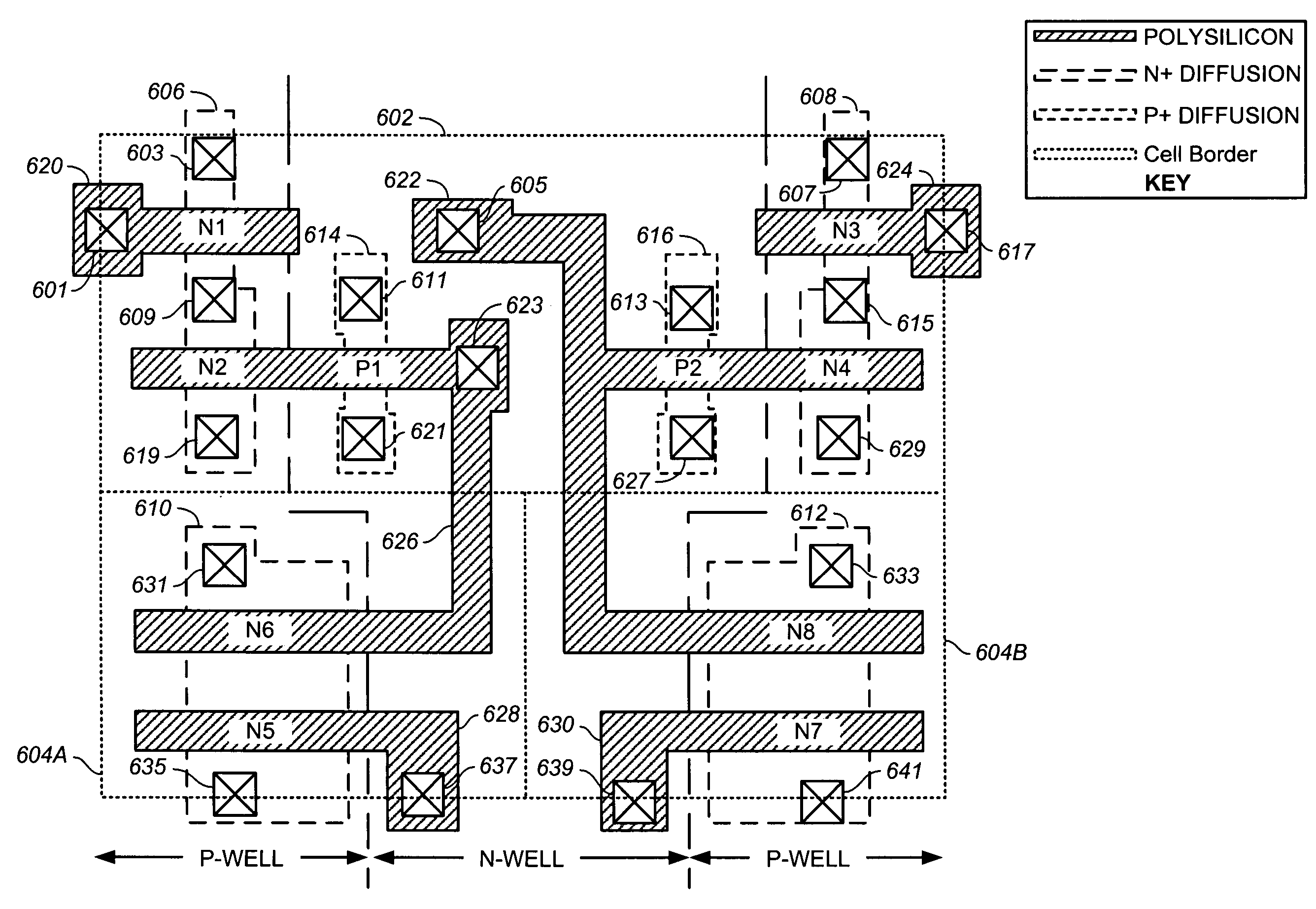
[0042]A binary CAM (BCAM) layout is shown in FIGS. 6A and 6B, with FIG. 6A showing the diffusion regions and gate lines and FIG. 6B demonstrating the metal-1, metal-2, and metal-3 layers. For reference between the two drawings, the contacts to the substrate are shown in both drawings. Additionally, each cell is divided by dotted lines into the 6T-SRAM 602 and comparison cells 604A, 604B. With reference first to FIG. 6A, shown are n-type diffusion regions 606, 608, 610, 612 and p-type diffusion regions 614, 616. There are six separate polysilicon gate lines 620, 622, 624, 626, 628, 630. Of these, gate line 620 forms the gate of transistor N1; gate line 622 forms the gate of transistors P2, N4, and N8; gate line 624 forms the gate of transistor N3; gate line 626 forms the gate line of transistors N2, P1, and N6; gate line 628 forms the gate of tr...


PUM


Abstract

Improved layouts of binary and ternary content addressable memory cells (BCAM and TCAM) are shown. A content addressable memory cell layout has a plurality of P+ diffusion areas and a plurality of N+ diffusion areas that do not enclose isolation regions and on which shallow trench isolation stress can exert minimal influence on the drive current of the memories. Further, all transistors in the content addressable memory cell layout are oriented in the same direction to avoid unintended variations in electrical performance. The CAM layouts are “process friendly” to accommodate requirements of advanced process technologies such as the 90 nm process.

Description

BACKGROUND OF THE INVENTION[0001]1. Technical Field[0002]The present invention relates generally to the data processing field and, more particularly, to layouts of ternary and binary content addressable memory cells for a data processing system.[0003]2. Description of the Related Art[0004]Content addressable memory (CAM) is a specialized type of memory. Unlike random access memory (RAM), where one uses a given address to randomly access the data stored there, CAM has the capability to supply an address, based on the value stored at or associated with the address. Additionally, an array of CAM cells will have built-in comparison circuitry for every cell of hardware memory. This allows a massively parallel search, where every bit in memory is searched simultaneously. Consequently, the hardware can provide an extremely fast search of a large set of information.[0005]This makes CAMs suitable for applications where fast searches are required, such as imaging, voice recognition, and netwo...

Claims


Application Information

Patent Timeline
Patent Type & Authority Patents(United States)
IPC IPC(8): G11C15/00
CPCG11C15/04H01L27/1104H01L27/11H10B10/00H10B10/12
Inventor VENKATRAMAN, RAMNATHCASTAGNETTI, RUGGEROGLENN, JOSEPH EUGENE
Owner AVAGO TECH WIRELESS IP SINGAPORE PTE
Why Eureka
Try Eureka