Self correcting data re-timing circuit and method

Active Publication Date: 2007-12-11
MARVELL ASIA PTE LTD
View PDF1 Cites 31 Cited by
  • Summary
  • Abstract
  • Description
  • Claims
  • Application Information

AI Technical Summary

Benefits of technology

[0033]Another broad aspect of the invention provides an eye opener circuit having a phase detector and data re-timer adapted to compare an input data signal to a locally generated clock signal to produce a phase error signal, and to sample the data signal using the locally generated clock signal to generate a sequence of samples, and to generate a new re-timed data signal having l

Problems solved by technology

However, by integrating the SERDES devices within the line card, the 10 Gbps serial data would then have to be transmitted from the line card to the optical module and this introduces jitter into the signal.
The deterministic component is generally caused by bandwidth limitations in the system and is typically data dependent, in the form of ISI (inter-symbol interference).
Other processes that can effect or introduce phase noise include crosstalk from other noise sources and power supply noise.
Systems specifications typically impose rather strict limitations on the amount of jitter that can be generated and injected into optical data being transmitted by the optical module.
There are also jitter limitations that apply to the electrical circuits used to drive the optical lasers or optical modulators used for transmission.
These limitations lead to the requirement for the bandwidth o

Method used


Image

  • Self correcting data re-timing circuit and method
  • Self correcting data re-timing circuit and method
  • Self correcting data re-timing circuit and method

Examples


Embodiment Construction

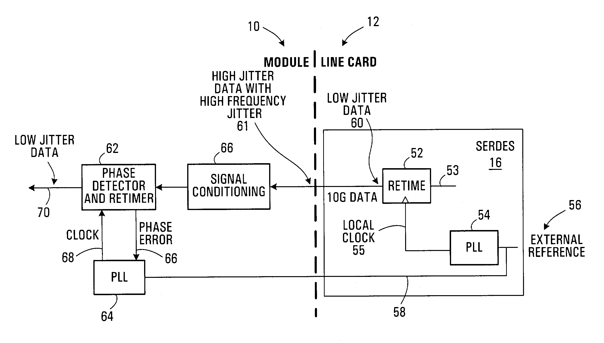
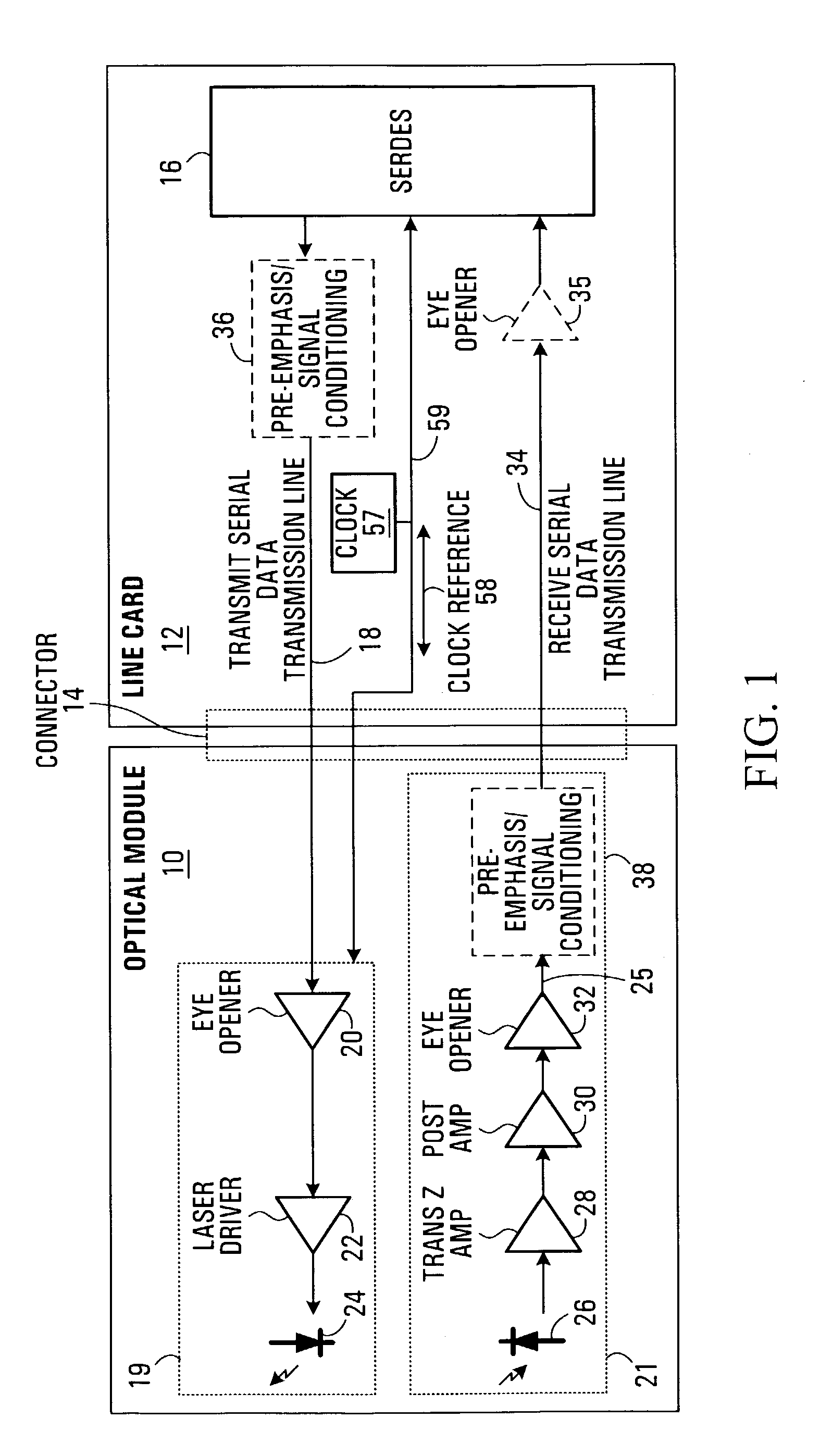
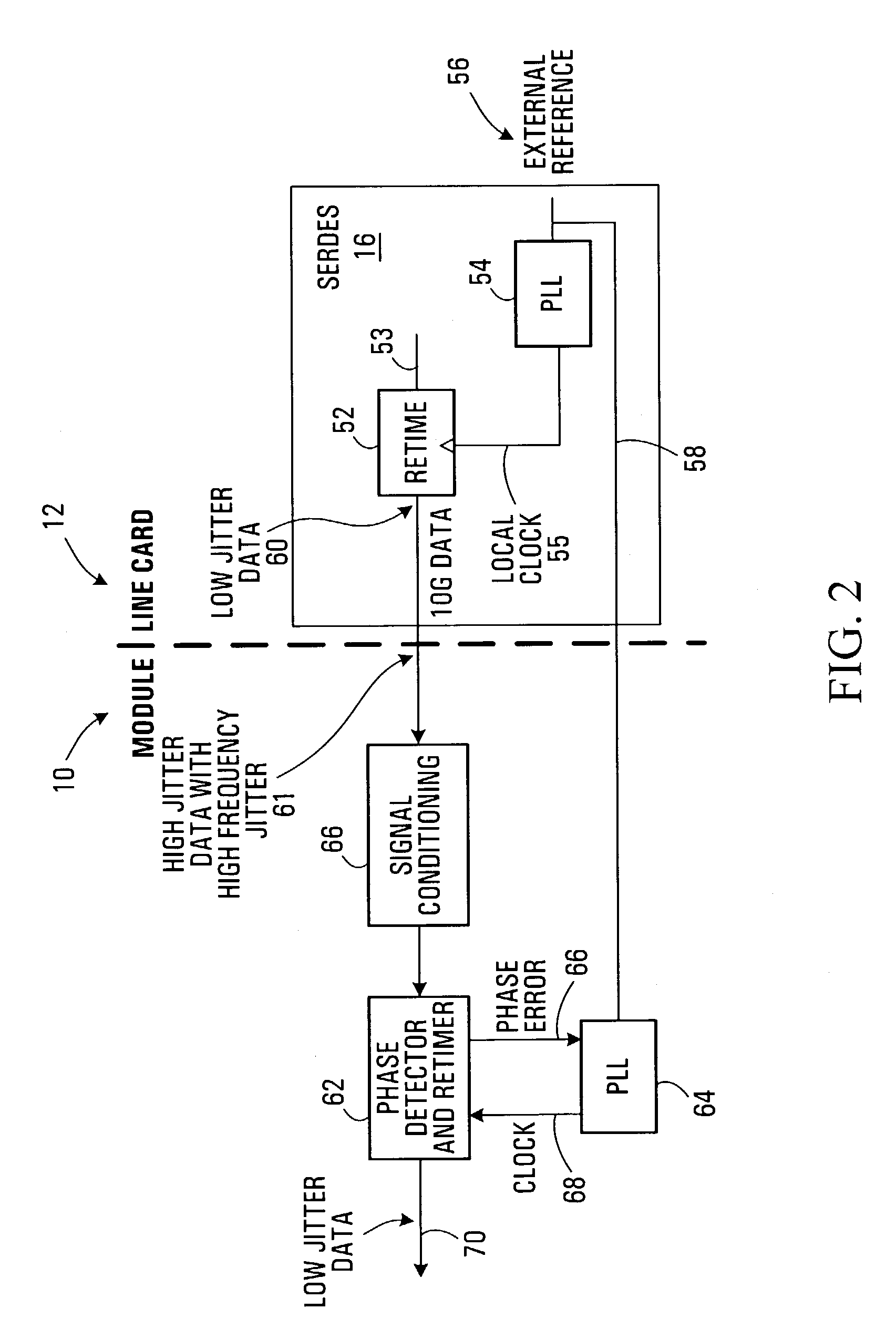
[0040]Referring to FIG. 1 an optical module 10 is shown connected to a line card 12 via a connector 14.

[0041]The electronic components of the line card 12 are placed atop a lossy PCB (Printed Circuit Board) substrate onto which conductive tracks are fabricated. For the purposes of the present description a SERDES device 16 is shown on the line card driven by a clock 57 which generates clock reference 58. Two conductive tracks 18, 34 from the SERDES 16 to the connector 14 are also shown. Also shown is a connection 59 through the connector 14 from the clock 57 providing the clock reference 58 to the optical module. An eye opener circuit 35 is shown on the receive path. Because standard specifications tend to be less stringent on the receive path, it is not necessary in all implementations to include this eye opener circuit 35. Some implementations might include a pre-emphasis / signal conditioning function 36. This would likely be implemented as part of the SERDES 16. More generally, it...


PUM


Abstract

An eye opener circuit is provided which performs a data re-timing/eye opening function on a data signal after having been corrupted by jitter. The circuit uses a PLL driven by a clock source which was the same clock source used in timing the data signal originally. The PLL generates a local clock used to re-time the data. A phase error may be introduced into the PLL, or into the data signal.

Description

RELATED APPLICATION[0001]This application claims the benefit of U.S. Provisional Application No. 60 / 359,709 filed Feb. 27, 2002.FIELD OF THE INVENTION[0002]The present invention relates generally to the field of data transmission. More particularly, the invention pertains to a method of reducing jitter (phase noise in the frequency domain) for data transmitted over a bandwidth-limited medium.BACKGROUND OF THE INVENTION[0003]Communication system providers that design and build data networks continue to provide new equipment that enables operators to provide higher data bandwidths to their customers. At the same time, operating companies purchasing the networking equipment prefer the equipment to be modular, such that the overall communication system is a combination of components that can be easily interchanged and interconnected. Additionally, it is desirable that each new generation of products enables increased data bandwidth in the same size time domain frame as their lower bandw...

Claims


Application Information

Patent Timeline
IPC IPC(8): H04L7/00
CPCH03L7/081H04L7/033H03L7/18
Inventor WALL, BRIANSCOUTEN, SHAWNSUZUKI, KENJISTEVENS, MALCOLM
Owner MARVELL ASIA PTE LTD
Why Eureka
Try Eureka