Semiconductor device

a technology of semiconductor devices and diodes, which is applied in the direction of semiconductor devices, semiconductor/solid-state device details, electrical apparatus, etc., can solve the problems of increased leakage current in the pn junction diode, prone to malfunction, and conventional pn junction diodes with a drawback of increasing leakage current, so as to reduce the leakage current through the junction

Inactive Publication Date: 2007-12-18
LAPIS SEMICON CO LTD
View PDF9 Cites 14 Cited by
  • Summary
  • Abstract
  • Description
  • Claims
  • Application Information

AI Technical Summary

Benefits of technology

[0016]According to the semiconductor device of the invention, the surface for the PN junction is only a bottom of the polysilicon plug, or the PN junction is formed in a contact surface between a diffusion layer in the surface of the silicon wafer and the polysilicon plug having a different conductive type from that of the diffusion layer, thereby flow direction of the electric current can be controlled one-way and the leakage current through the junction can be reduced.

Problems solved by technology

Generally, since the electric current that flows through the circuit increases with increase of the junction area, the large junction area causes increase of leakage current in the PN junction diode.
Thus, the conventional PN junction diode has a drawback of increase of the leakage current because the diode has many current flow paths and a large junction area.
That is, the charge-up current generated in the plasma treatment such as sputtering in formation of the wiring connected to the PN junction diode flows in many directions, thereby malfunction is apt to occur.

Method used


Image

  • Semiconductor device
  • Semiconductor device
  • Semiconductor device

Examples


Embodiment Construction

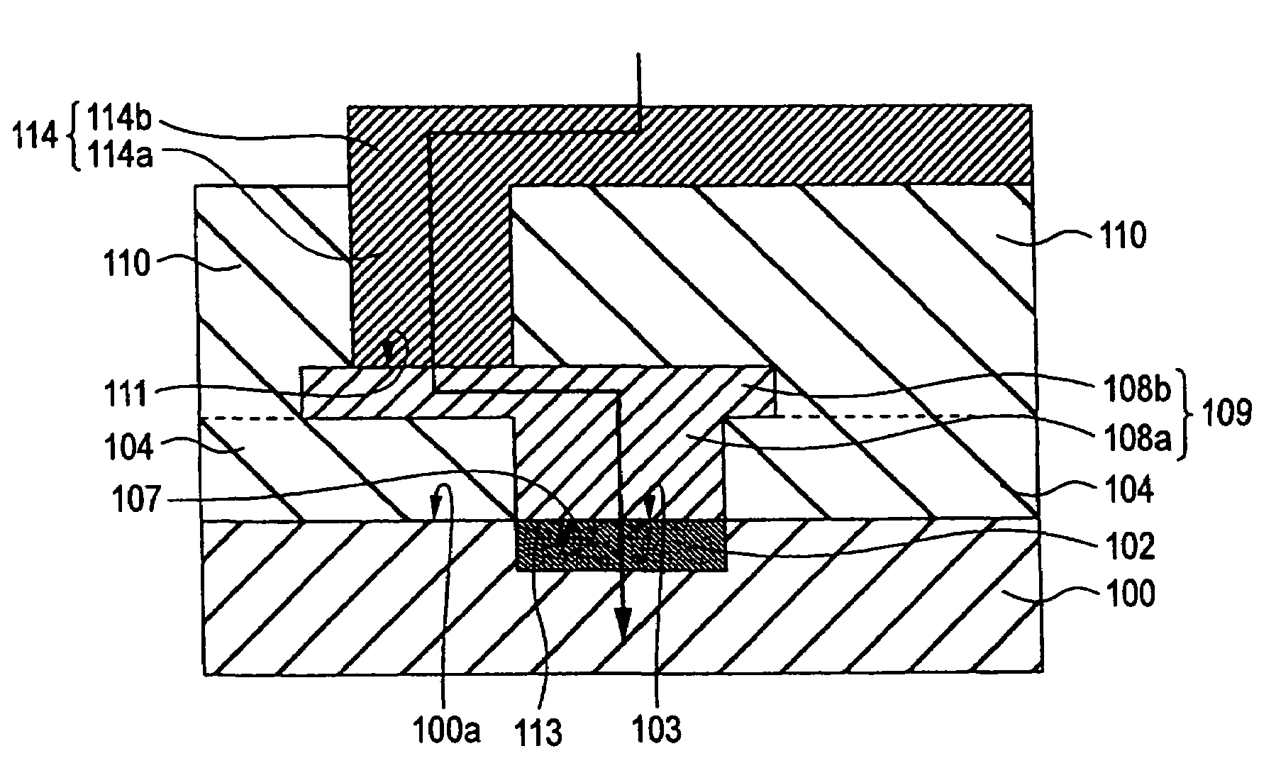
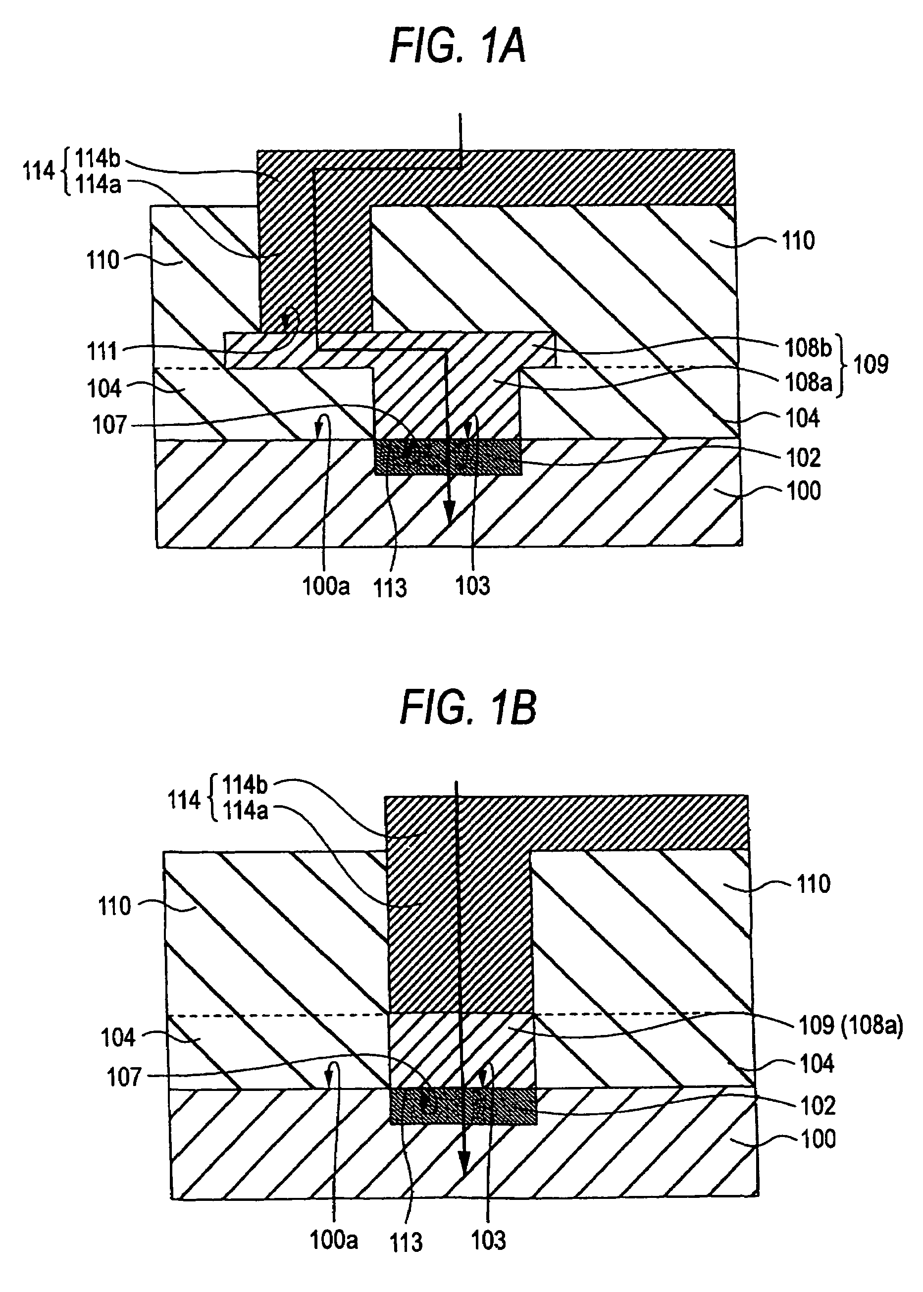
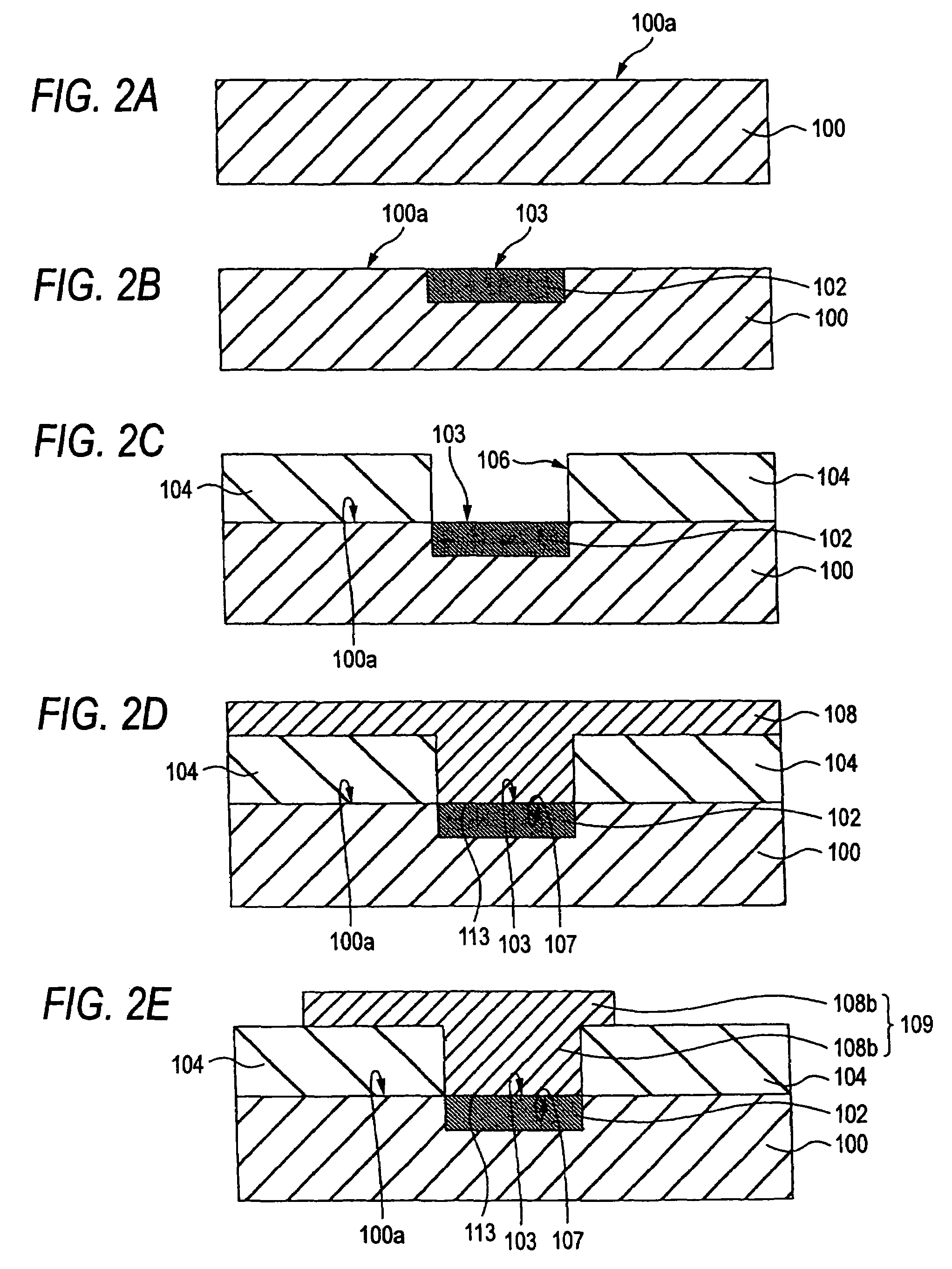
[0023]Hereinafter, the best mode for practicing the invention is described with reference to drawings. Respective drawings for describing the production method schematically show sections of structures obtained in respective steps of the production process. Size, shape, and arrangement of each component forming the structures are shown schematically in such a degree that the invention can be briefly understood. Similar components in respective drawings are marked with the same numerals, and an overlapped description of the components may be omitted.

[0024]Hereinafter, a case of a PN junction diode in which a P+ polysilicon plug as the second conductive type polysilicon plug provided in contact with the upper surface of the first conductive type impurity region is formed on the N+ region as the first conductive type impurity region provided with the upper surface being exposed on one main surface of a silicon (Si) substrate is described as an example. Accordingly, the N-type correspon...


PUM


Abstract

Leakage current generated in a PN junction diode is reduced, and charge-up current caused by plasma treatment in formation of wiring connected to the PN junction diode is controlled. An N+ region as a first conductive type impurity region provided in a Si substrate with an upper surface being exposed on one main surface of the Si substrate, a P+ polysilicon plug provided with a bottom being contacted with an upper surface of the N+ region, and wiring connected to a top of the P+ polysilicon plug are included.

Description

BACKGROUND OF THE INVENTION[0001]1. Field of the Invention[0002]The present invention relates to a semiconductor device, particularly, a semiconductor device having metal wiring connected to a diode having a PN junction.[0003]2. Description of the Related Art[0004]In a conventional semiconductor device, as the diode having the PN junction (hereinafter, referred to as PN junction diode) and metal wiring connected to the PN junction diode, those having the following structures are included.[0005]FIG. 4A shows a section of a schematic structure of the conventional PN junction diode and the metal wiring connected to the PN junction diode.[0006]A P+ region 204 for forming the PN junction is formed in an N+ region 202 formed on a surface of a Si substrate 200. A conductive layer plug 210a is formed on the P+ region 204 and connected to a conductive layer wiring 210b. The conductive layer plug 210a and the conductive layer wiring 210b are formed from a metal such as aluminum, and the condu...

Claims


Application Information

Patent Timeline
Patent Type & Authority Patents(United States)
IPC IPC(8): H01L29/06H01L21/28H01L21/329H01L29/417H01L29/861
CPCH01L29/861H01L29/417
Inventor FUKURO, TAKETO
Owner LAPIS SEMICON CO LTD
Why Eureka
Try Eureka