Driving circuit of a semiconductor display device and the semiconductor display device

a driving circuit and display device technology, applied in static indicating devices, instruments, optics, etc., can solve the problems of above described problems, display blur (display unevenness) of the display device as a whole, change of threshold value or deterioration, etc., to eliminate picture blur, excellent picture, and high fineness/high resolution

Inactive Publication Date: 2008-01-01
SEMICON ENERGY LAB CO LTD
View PDF87 Cites 27 Cited by
  • Summary
  • Abstract
  • Description
  • Claims
  • Application Information

AI Technical Summary

Benefits of technology

[0013]The present invention has been made to overcome the foregoing problems, and an object thereof is to provide a semiconductor display device which can eliminate picture blur (display unevenness) and can obtain an excellent picture with high fineness / high resolution.
[0014]According to a mode of carrying out the present invention, in a driving circuit of a semiconductor display device, as a TFT constituting a buffer circuit provided between a shift register circuit and a latch circuit of a source signal line side driving circuit, a TFT having a large size (channel width) is not used, but instead thereof, a plurality of TFTs each having a small size and are connected in parallel with each other are used. Moreover, as a TFT constituting a buffer circuit provided between a shift register circuit and a gate signal line of a gate signal line side driving circuit, a TFT having a large size (channel width) is not used, but instead thereof, a plurality of TFTs each having a small size and are connected in parallel with each other are used. In both cases, a plurality of buffer circuits are connected in parallel with each other to constitute a buffer circuit portion in a driver circuit. By doing so, it is possible to reduce fluctuation in characteristics of the buffer circuit while securing the current capacity thereof.

Problems solved by technology

This causes display blur (display unevenness) of the display device as a whole.
Further, when the size of a TFT is large, self heat generation of the TFT becomes large, which sometimes causes change of a threshold value or deterioration.
Also in this case, since a buffer having a large current capacity becomes necessary, the above described problems come to occur.
Especially, the buffer of the gate signal line must drive all of the connected TFTs for one line in the pixel matrix circuit, so that the fluctuation in the characteristics of the buffer makes remarkable picture unevenness.
This is one of the most serious problems when a display device with high fineness / high resolution is desired.

Method used


Image

  • Driving circuit of a semiconductor display device and the semiconductor display device
  • Driving circuit of a semiconductor display device and the semiconductor display device
  • Driving circuit of a semiconductor display device and the semiconductor display device

Examples


embodiment 1

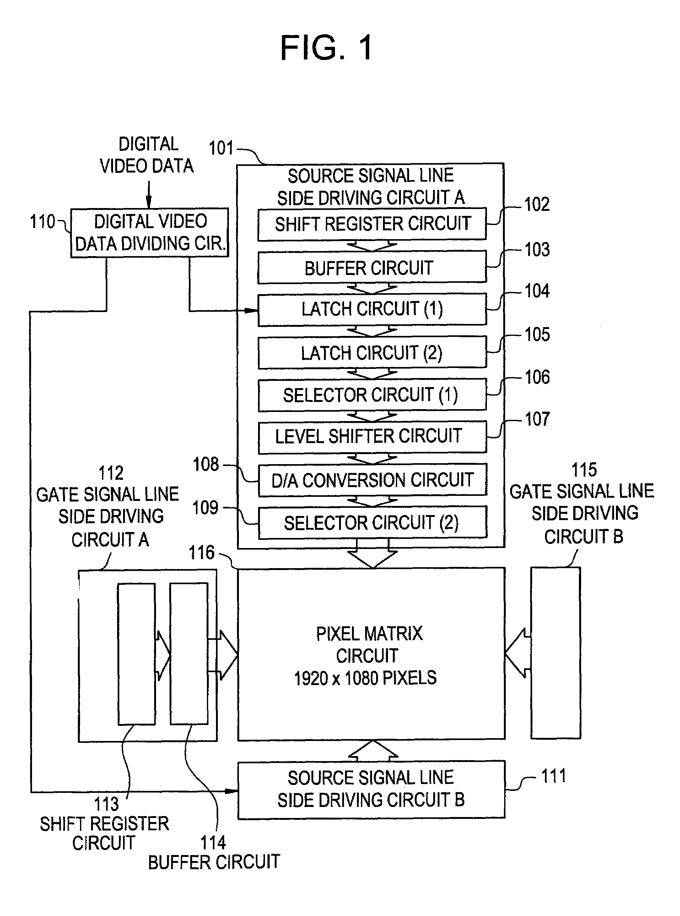
[0040]In this embodiment, as an example in which a driving circuit of a semiconductor display device of the present invention is used, an active matrix type liquid crystal display device in which the number of pixels is 1920×1080 in horizontal and vertical will be described.

[0041]Reference will be made to FIG. 1. FIG. 1 is a block diagram of a main portion of an active matrix type liquid crystal display device of this embodiment. The active matrix type liquid crystal display device of this embodiment includes a source signal line side driving circuit A 101, a source signal line side driving circuit B 111, a gate signal line side driving circuit A 112, a gate signal line side driving circuit B 115, a pixel matrix circuit 116, and a digital video data dividing circuit 110.

[0042]The source signal line side driving circuit A 101 includes a shift register circuit 102, a buffer circuit 103, a latch circuit (1) 104, a latch circuit (2) 105, a selector circuit (1) 106, a level shifter circu...

embodiment 2

[0188]In the foregoing embodiment 1, description has been made on the case where the digital driving system driving circuit of the present invention is used for the active matrix type liquid crystal display device. In this case, as a display method used for the active matrix type liquid crystal display device, a TN mode using a nematic liquid crystal, a mode using electric field control birefringence, a mixed layer of a liquid crystal and a high polymer, a so-called polymer dispersion mode, and the like can also be used.

[0189]Further, in the digital driving system driving circuit of the present invention, the line-sequential scanning of the pixel TFTs is carried out as described above, and the number of pixels corresponds to the future ATV (Advanced TV). Thus, if the driving circuit is used for an active matrix type liquid crystal display device which uses a liquid crystal with a high response speed, that is, a so-called non-threshold antiferroelectric liquid crystal, more excellent...

embodiment 3

[0193]In the embodiments 1 and 2, although a transmission type active matrix liquid crystal display device has been described, it is needless to say that the driving circuit of the present invention can also be used for a reflection type active matrix liquid crystal display device.


PUM

PropertyMeasurementUnit
widthsaaaaaaaaaa
widthaaaaaaaaaa
widthaaaaaaaaaa

Abstract

There are provided a driving circuit of a semiconductor display device which can obtain an excellent picture without picture blur (display unevenness) and with high fineness / high resolution, and the semiconductor display device. A buffer circuit used in the driving circuit of the semiconductor display device is constituted by a plurality of TFTs each having a small channel width, and a plurality of such buffer circuits are connected in parallel with each other.

Description

BACKGROUND OF THE INVENTION[0001]1. Field of the Invention[0002]The present invention relates to a driving circuit of an active matrix type semiconductor display device. The present invention also relates to the semiconductor display device having the driving circuit.[0003]2. Description of the Related Art[0004]In recent years, a technique for manufacturing a semiconductor device having a semiconductor thin film formed on an inexpensive glass substrate, such as a thin film transistor (TFT), has been rapidly developed. The reason is that the demand for an active matrix type semiconductor display device (especially an active matrix type liquid crystal display device) has been increased.[0005]In the active matrix type liquid crystal display device, a TFT is disposed for each of several tens to millions of pixels arranged in matrix, and an electrical charge going in and out each pixel electrode is controlled by a switching function of the TFT.[0006]Especially, with the improvement of a ...

Claims


Application Information

Patent Timeline
Patent Type & Authority Patents(United States)
IPC IPC(8): G09G3/36G02F1/133G02F1/1345G02F1/1368G09G3/20G09G3/30H01L21/82H01L21/822H01L27/04H01L29/786H01L51/50H05B33/14
CPCG09G3/3674G09G3/3688G09G3/3648G09G3/32G09G3/3611G09G2300/0408G09G2310/027G09G2320/0233H01L27/1214G09G2310/0286
Inventor KOYAMA, JUNYAMAZAKI, SHUNPEI
Owner SEMICON ENERGY LAB CO LTD
Why Eureka
Try Eureka