Fin FET structure

a technology of fin fet and active region, which is applied in the direction of transistors, semiconductor devices, electrical equipment, etc., can solve the problems of gate induced drain leakage (gidl), junction leakage current not distinctly improved, difficult control of threshold voltage, etc., to improve the swing characteristics of transistors, reduce or prevent leakage current in channels, and improve the effect of transistor refresh characteristics

Active Publication Date: 2008-01-08
SAMSUNG ELECTRONICS CO LTD
View PDF18 Cites 88 Cited by
  • Summary
  • Abstract
  • Description
  • Claims
  • Application Information

AI Technical Summary

Benefits of technology

[0009]Exemplary embodiments of the invention provide a fin FET structure using a bulk silicon substrate or an SOI silicon substrate, in which a negative bias is applied to a gate electrode under an off state of fin FET by using a negative word line scheme, thereby substantially reducing or preventing a leakage current in a channel and maintaining an off state of the channel. The structure increases a threshold voltage of the fin FET by using a gate electrode with an n+ impurity-doped electrode, without performing a channel doping for a control of threshold voltage or with performing the channel doping by a low density, thereby improving swing characteristics of the transistor and refresh characteristics. The structure also substantially reduces a junction leakage current between a storage node and a substrate, and a gate induced drain leakage (GIDL), with enhancing characteristics of the transistor.

Problems solved by technology

However, when the fin active region is less than 100 nm, the threshold voltage is difficult to control compared to a planar-type transistor or a recess-type transistor.
Furthermore, a leakage current is generated in an off state of the fin FET, and a gate induced drain leakage (GIDL) and a junction leakage current are not distinctly improved compared to the planar type transistor and the recess type transistor.

Method used


Image

  • Fin FET structure
  • Fin FET structure
  • Fin FET structure

Examples


Embodiment Construction

[0021]Exemplary embodiments of the invention are more fully described in detail with reference to the accompanied drawings. The invention may be embodied in many different forms and should not be construed as being limited to the exemplary embodiments set forth herein. Rather, these exemplary embodiments are provided so that this disclosure is thorough and complete, and to convey the concept of the invention to those skilled in the art.

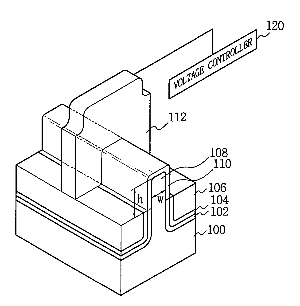
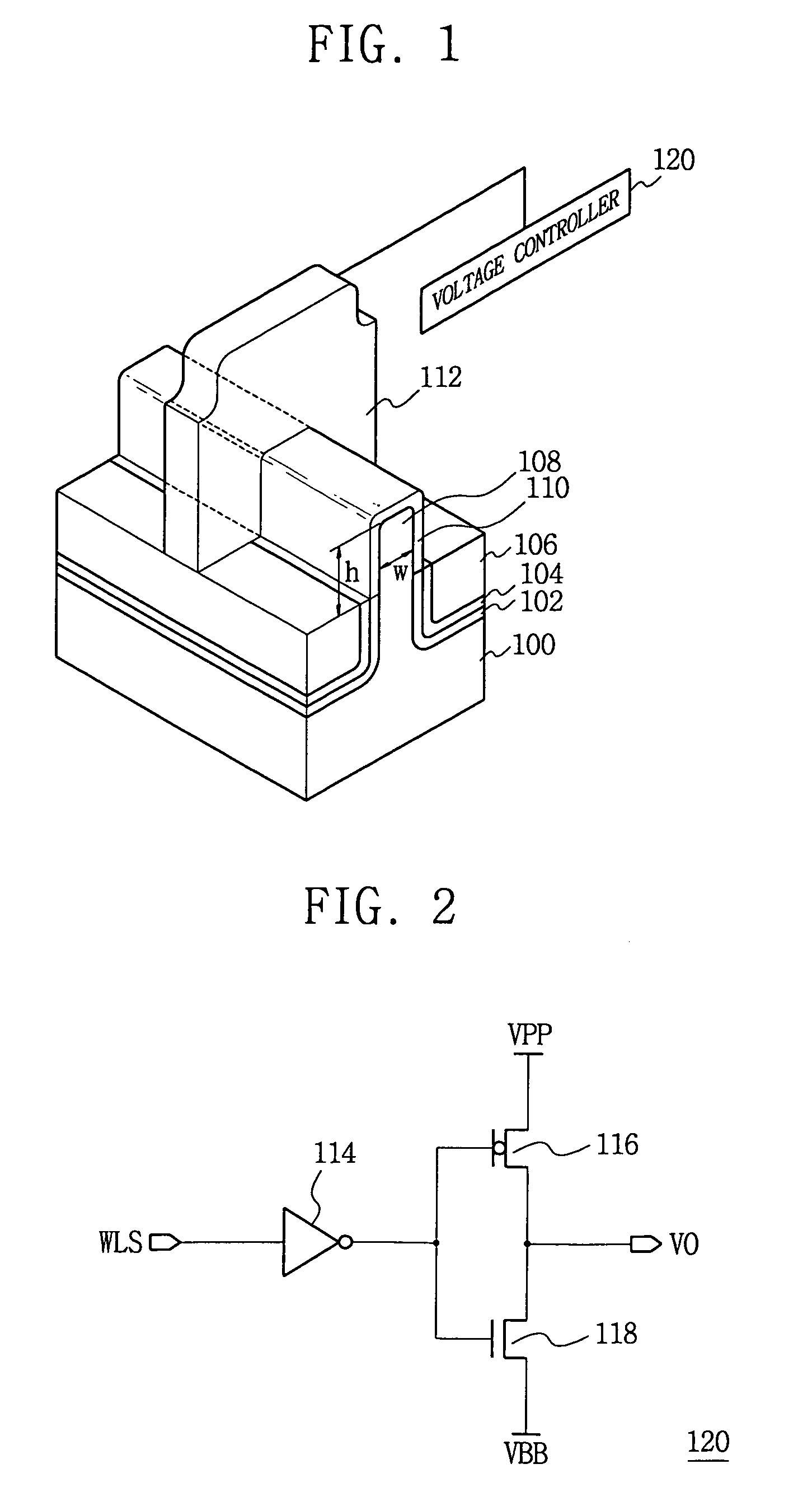
[0022]FIG. 1 is a perspective diagram illustrating a fin FET according to some embodiments of the invention. FIG. 2 is a circuit diagram illustrating an exemplary voltage controller suitable for use with the fin FET of FIG. 1. The voltage controller will be described in relation to a write operation of a DRAM cell in using an inventive fin FET as a cell array transistor.

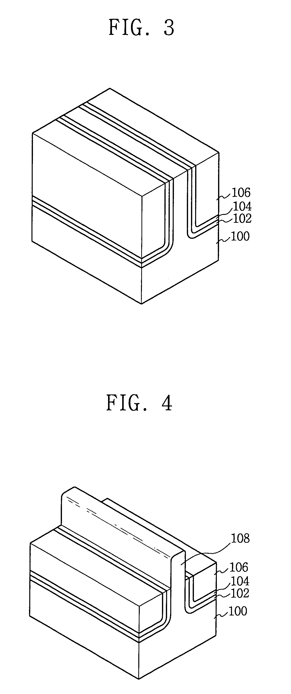
[0023]Referring to FIGS. 1 and 2, a semiconductor substrate 100 of a first conductive type is provided, and a fin active region 108 of a first conductive type extends from an upper sur...


PUM


Abstract

A fin FET structure employs a negative word line scheme. A gate electrode of a fin FET employs an electrode doped with n+ impurity, and a channel doping for a control of threshold voltage is not executed, or the channel doping is executed by a low density, thereby remarkably improving characteristics of the fin FET. A semiconductor substrate is formed in a first conductive type, and a fin active region of a first conductive type is projected from an upper surface of the semiconductor substrate and is connected to the semiconductor substrate. An insulation layer is formed on the semiconductor substrate, and a gate insulation layer is formed in upper part and sidewall of the fin active region. A gate electrode is formed on the insulation layer and the gate insulation layer. Source and drain are formed in the fin active region of both sides of the gate electrode.

Description

CROSS REFERENCE TO RELATED APPLICATIONS[0001]This application claims priority from Korean Patent Application No. 2004-8598, filed on Feb. 10, 2004, the content of which is hereby incorporated by reference in its entirety for all purposes.BACKGROUND OF THE INVENTION[0002]1. Field of the Invention[0003]This disclosure relates to a semiconductor memory device, and more particularly, to a fin Field Effect Transistor (FET) having a fin type active region.[0004]2. Description of the Related Art[0005]As the trend to achieve semiconductor memory devices having low power, high efficiency, and high speed characteristics continues, a design rule is continuously reduced to integrate more semiconductor memory devices into a semiconductor chip of limited size. In particular, in a highly integrated DRAM (Dynamic Random Access Memory) device, a design rule may be 100 nm, thus an interval from a gate is gradually reduced, generating a short channel effect and increasing the channel doping density of...

Claims


Application Information

Patent Timeline
Patent Type & Authority Patents(United States)
IPC IPC(8): H01L29/94H01L27/108H01L21/336H01L21/8242H01L29/49H01L29/78H01L29/786H01L31/062
CPCH01L29/4908H01L29/66795H01L29/785H01L29/7854H01L21/18
Inventor LEE, CHOONG-HOPARK, DONG-GUNYOUN, JAE-MANLEE, CHUL
Owner SAMSUNG ELECTRONICS CO LTD
Why Eureka
Try Eureka