Photovoltaic conversion device and method of manufacturing the device

a technology of photovoltaic conversion and manufacturing method, which is applied in the direction of radiation control devices, sustainable manufacturing/processing, and final product manufacturing, etc., can solve the problems of reducing affecting the efficiency of solar cells, and affecting the quality of crystalline silicon grains in bottom and side portions of ingots with which they are in contact, etc., to achieve high photovoltaic conversion properties, reduce the number of steps, and achieve strong gettering effect

Inactive Publication Date: 2008-01-08
KYOCERA CORP
View PDF2 Cites 34 Cited by
  • Summary
  • Abstract
  • Description
  • Claims
  • Application Information

AI Technical Summary

Benefits of technology

[0044]As described above, since the photovoltaic conversion device according to the present invention is arranged such that a minority carrier diffusion length in the bulk surface region comprising a light active region is a certain value (½ or more of Lpeak), it is possible to reduce adverse influence of impurities such as Fe contained in the bulk surface region on the photovoltaic conversion properties. In addition, it is possible to reduce adverse influence of Fe and the like on the photovoltaic conversion properties in a wide area of the substrate.
[0061]Additionally, the steps of heat treatment of the first and second n-type regions may be carried out simultaneously. This allows the number of steps to be reduced.

Problems solved by technology

Metals, in particular, transition metals are typical factors that degrade the properties of solar cells.
That is, crystalline silicon grains in bottom and side portions of an ingot with which they are in contact have extremely low quality.
However, it is not necessarily easy.
This is because significant purification of the starting material and components leads to higher costs, it is not technically easy, and a certain degree of impurity mixing is inevitable in the process.
The foregoing conventional P gettering effect that is additionally utilized for pn junction formation in photovoltaic conversion devices is not necessarily sufficient.
However, this is not enough to extract a maximum P gettering effect.
However, in order to fully extract gettering effect, only considering the distance index is not sufficient.
While the concentration and thickness of the P thermal diffusion region are important indices that affect the gettering effect, it has been difficult to achieve sufficient values of them in conventional P thermal diffusion processes in which the peak temperature is restricted and the time for the thermal diffusion is short for forming a shallow pn junction.
As a result, sufficient improvement in properties cannot be achieved.
Therefore, this region with insufficiently improved quality is a great factor that restricts improvement of properties.
If this part is disposed of as waste, the part of silicon material that is disposed of leads to an increase of cost, which is problematic.

Method used


Image

  • Photovoltaic conversion device and method of manufacturing the device
  • Photovoltaic conversion device and method of manufacturing the device
  • Photovoltaic conversion device and method of manufacturing the device

Examples


example

[0185]An advantageous effect of the present invention will be described referring to a bulk multicrystalline silicon solar cell element fabricated according to the embodiment above.

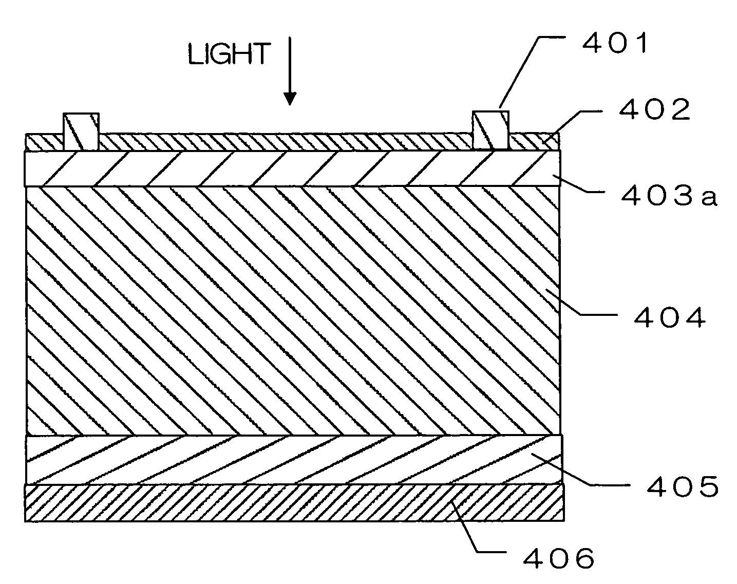
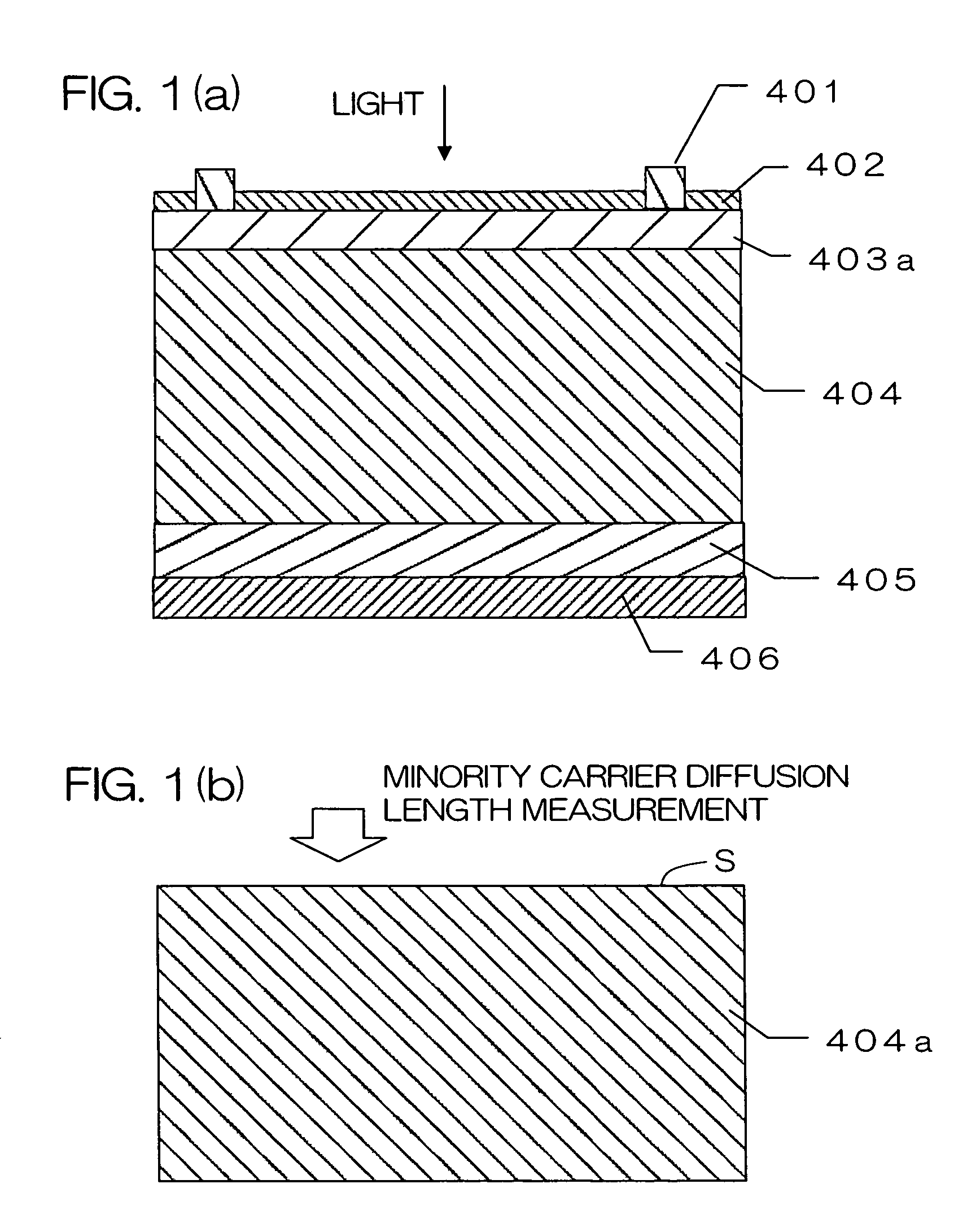
[0186]The substrate was-selected among multicrystalline silicon substrates produced by casting to be substrates shown in FIGS. 3 and 4 that have the low quality substrate peripheral regions originating from a side portion of the ingot with characteristic crystal grain configurations, which were used as the boron-doped p-type multicrystalline silicon substrate.

[0187]The dimensions of the substrate were 15 cm square and thickness thereof was 300 μm.[0188]1) Minority carrier diffusion length of the substrate before processing for a solar cell element (before application of the present invention).

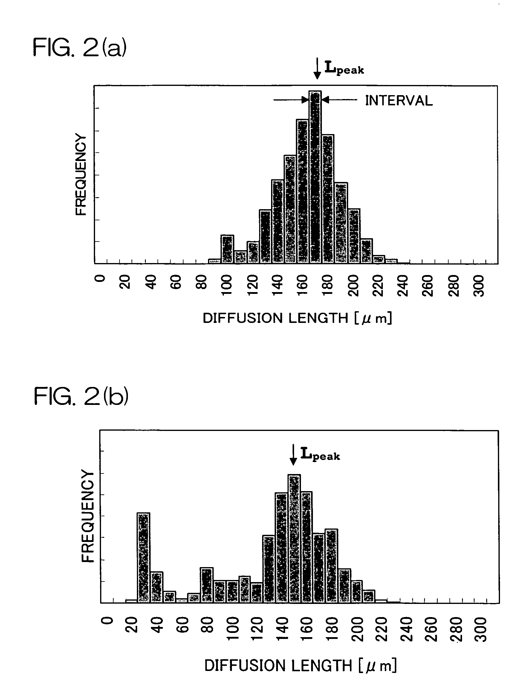
[0189]First, measurements of minority carrier diffusion lengths of these multicrystalline silicon substrates (before processing) were carried out. The measurement apparatus used was a SPV apparatus (Cat. No. FAaST210...


PUM

PropertyMeasurementUnit
minority carrier diffusion lengthaaaaaaaaaa
minority carrier life timeaaaaaaaaaa
temperatureaaaaaaaaaa

Abstract

There is disclosed a photovoltaic conversion device constructed using a p-type crystalline silicon substrate 404 doped with boron, which comprises a bulk substrate region 404, regions other than the bulk substrate region including an n-type region 403a joining to a light receiving surface of the bulk surface region, a BSF region 405 joining to a back surface of the bulk surface region,wherein with regions other than the bulk substrate region 404 being removed, when a minority carrier diffusion length of the bulk substrate region 404 is measured from the light receiving surface of the bulk surface region, 0.5<(L1 / Lpeak)is satisfied, where L1 is a minority carrier diffusion length at an arbitrary measuring area of the light receiving surface of the bulk surface region, and Lpeak is a diffusion length corresponding to a maximum peak on the side of higher diffusion length of a histogram, the histogram being formed from data obtained when a minority carrier diffusion length of the light receiving surface of the bulk surface region is measured at a plurality of measurement areas. This structure can reduce influence of impurities such as Fe, and enhances utilization efficiency of silicon ingots. With this structure, a photovoltaic conversion device with high photovoltaic conversion efficiency can be realized.

Description

BACKGROUND OF THE INVENTION[0001]1. Field of the Invention[0002]The present invention relates to photovoltaic conversion devices represented by solar cells, and in particular, to a photovoltaic conversion device in which the properties thereof is improved by reducing influence of impurities mixing into during the manufacture thereof.[0003]2. Description of the Related Art[0004]In the specification, “aEn” represents “a×10n”.[0005]Bulk photovoltaic conversion devices using multicrystalline silicon substrates now occupy a major part of the market of solar cells.[0006]Generally, multicrystalline silicon substrates are manufactured by a casting method. However, a number of metal elements are included as impurities in the multicrystalline silicon substrates that are sliced out of a multicrystalline silicon ingot produced by the casting method.[0007]Metals, in particular, transition metals are typical factors that degrade the properties of solar cells. Therefore, reducing the influence the...

Claims


Application Information

Patent Timeline
Patent Type & Authority Patents(United States)
IPC IPC(8): H01L31/06C30B9/00C30B11/00C30B17/00C30B21/02C30B28/06H01L31/036H01L31/04H01L31/042H01L31/068H01L31/18
CPCH01L31/186Y02E10/50Y02E10/546Y02P70/50
Inventor NIIRA, KOICHIROGOTOH, SHIGERU
Owner KYOCERA CORP
Why Eureka
Try Eureka