Product identification tag device and reader

a product identification and tag technology, applied in the field of electronic reading identification tags, can solve the problems of large amount of energy required by the reader, large application range, and large antenna, and achieve the effects of optimizing efficiency and performance, minimizing rf interference, and maximizing tag power absorption

Inactive Publication Date: 2008-01-08
TAGENT
View PDF8 Cites 148 Cited by
  • Summary
  • Abstract
  • Description
  • Claims
  • Application Information

AI Technical Summary

Benefits of technology

[0011]The invention described herein essentially optimizes the efficiency and performance of a very small radio frequency identification tag that has a built-in antenna directly on the integrated circuit, as described in Pat. No. 6,480,699. In the invention power management is optimized, wherein RF emanating from a reader / transmitter is absorbed by a power supply circuit in an RF ID tag generally as in U.S. Pat. No. 6,480,699. In addition, problems of RF interference are minimized, componentry onboard the integrated circuit is kept to a minimum, tag power absorption is maximized and the operating range of the RF ID system is at the same time maximized, and the chip is protected from over voltages.
[0012]In one aspect of the invention, a signal transmitter in the tag's integrated circuit, powered by energy absorbed into the power supply, transmits a data signal containing the unique product information on a radio frequency which is distinctly different from that of the reader's transmitted power signal. This eliminates or minimizes interference between the reader (or power) signal and the data signal returned to the reader, eliminating the need for filters or other circuitry that would otherwise be required to interpret the data despite such interference.
[0013]The system minimizes power requirements for the tag by minimizing intelligence in the IC. The accuracy of the tag transmit frequency is assured in one embodiment by using a clock frequency generated by the reader, as a pulsing in the power signal, which is received in the tag and multiplied to the prescribed transmit frequency, rather than relying on onboard IC circuitry to assure the proper transmit frequency. In another embodiment the tag's frequency is generated using a 1% accuracy clock oscillator that is powered only when the tag is powered by the RF power signal.

Problems solved by technology

However, such reflective transponders in this type of identification tag require transmission of a large amount of energy from the reader, especially if the reader is to function at any practical distance, such as several meters.
Such an antenna is, therefore, potentially extremely small and possesses wide application.
In such an electronic transponder identification tag as described in the '699 patent, power management is a challenge.
The power can be gained incrementally by the power supply of the tag, over a period of time, but this time cannot be excessive or the system of readers / tags will not work effectively for many situations.
If the device is extremely small, such as to be embedded in thin items which might include paper money or other papers, the antenna is so small as to create further problems of power management, in that the antenna must both capture RF energy and transmit a sufficient signal to be received.
Also, the more electronic components that must be powered on the IC of the tag, the greater the power requirement, and thus further complications in power management.
Another issue relates to storing sufficient voltage in the tag's power supply for the tag to operate.
The small size of the tag and the small onboard antenna make this difficult in some circumstances, for a system which operates within FCC regulations.
A further issue can be voltage regulation at the tag to protect transistors onboard the chip from harmful high voltages that can be induced on the antenna.
Still another issue for the contemplated system is the potential for interference with other communications devices nearby.
Power storage is adversely affected, as is the ability to transmit the response.

Method used


Image

  • Product identification tag device and reader
  • Product identification tag device and reader
  • Product identification tag device and reader

Examples


Embodiment Construction

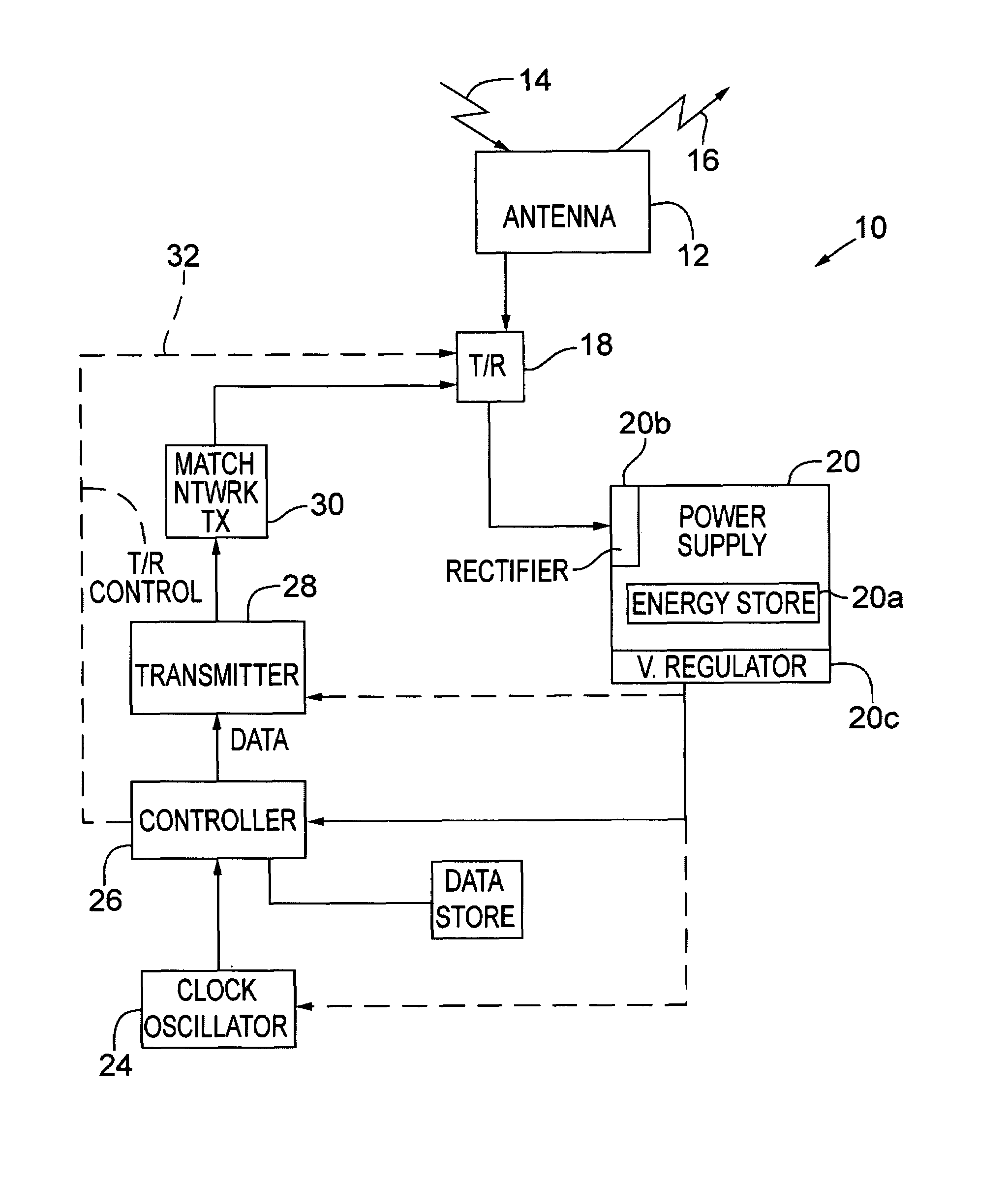
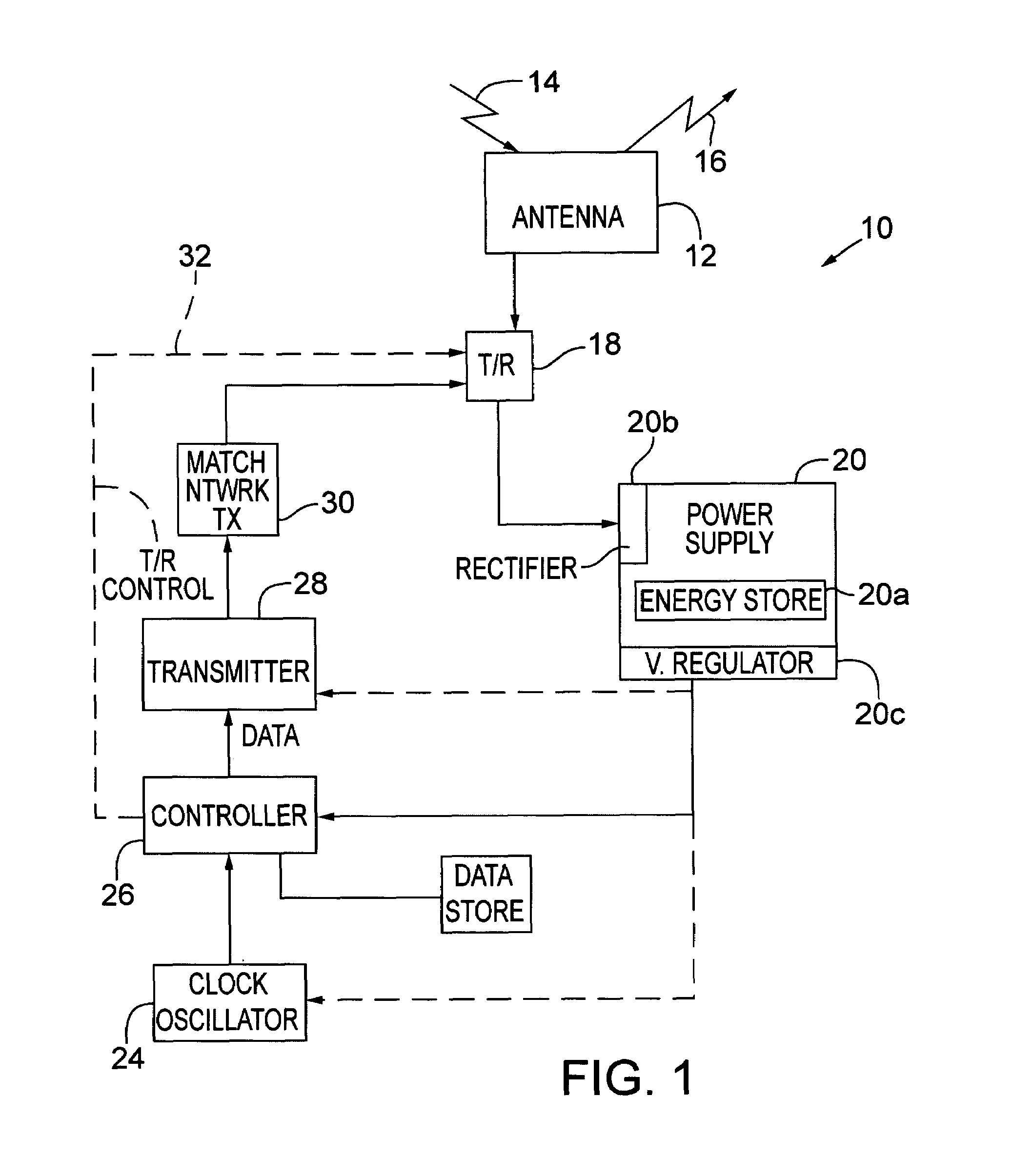
[0027]In the drawings, FIG. 1 illustrates, in a schematic block diagram, one embodiment of a circuit 10, shown simplified, that can be included on an RF ID tag according to the invention. In this embodiment, a single antenna 12 is formed on the chip, receiving power signals 14 and transmitting reply signals 16. The antenna is connected to a transmit / receive switch 18, which could also be a diplexer, so that when in receive mode the antenna conducts power pulses to a power supply 20 that preferably is a capacitive device as described in Pat. No. 6,480,699. A portion of the RF energy from the power signal 14 is captured and builds up over a period of time by capacitive storage in the power supply 20, which includes an energy store 20a for capacitive storage, as well as a rectifier 20b to produce DC current for the energy store, and a voltage regulator 20c to control output voltage from the power supply. Disclosure of these components is contained in the '699 patent, which is incorpora...


PUM


Abstract

An electronic identification tag, usually in very small size, responds to a reader with an identification code unique to the object to which the tag is attached. The stand-alone device responds to a reader signal by storing energy received from the signal, then using the stored energy to generate another signal that is encoded with identification information. In operation, a reader generates RF energy which can reach a multiplicity of such tags over a distance of several meters. The system minimizes power requirements for the tag by minimizing intelligence in the IC. Use of a transmit frequency which is different from the reader's power frequency reduces interference between the power pulse and information pulse, eliminates the need for filters and enables the multiplied clock reference frequency as the transmit carrier frequency.

Description

BACKGROUND OF THE INVENTION[0001]This invention concerns electronically readable identification tags for inventory control, automated sales, tracking shipped items, theft detection, counterfeit detection and other purposes, and more specifically the invention concerns particular embodiments of and enhancements to the ID tag device and reader system disclosed in U.S. Pat. No. 6,480,699. The invention provides for high efficiency in the receiving and storage of power in the tag device and in transmitting a signal from the tag essentially without interference from the reader signal.[0002]A number of identification tags have previously been proposed and used to electronically control, detect and track a variety of items to which these tags are attached. These are usually in the form of a card including an antenna. When affixed to or embedded into virtually any object, the tag can individually identify the object using a unique, factory-programmed unalterable code held in a memory mounte...

Claims


Application Information

Patent Timeline
Patent Type & Authority Patents(United States)
IPC IPC(8): H04Q1/00
CPCG06K7/0008G06K19/0701
Inventor JARVIS, NEILLOVOI, PAUL A.FAY, WARRENLEE, CHRISTOPHER J.BOLANDER, JARIE G.BARON, BERNARDJENNETTI, ANTHONY G.WUNDERLICH, FORRESTAYZENBERG, OSCAR
Owner TAGENT
Why Eureka
Try Eureka