Carbon nanotube-based field emission device

a carbon nanotube and emission device technology, applied in the manufacture of electric discharge tubes/lamps, discharge tubes luminescnet screens, electrode systems, etc., can solve the problems of reducing the uniformity and stability of electron emission from carbon nanotube bundles, unable to predict or control, and not being able to predict the effect of emission, etc., to achieve the effect of improving the uniformity and stability of electron emission

Active Publication Date: 2008-01-15
TSINGHUA UNIV +1
View PDF7 Cites 10 Cited by
  • Summary
  • Abstract
  • Description
  • Claims
  • Application Information

AI Technical Summary

Benefits of technology

[0007]Accordingly, an object of the present invention is to provide a carbon nanotubes-based field emission device having an improved uniformity and stability of electron emissions.
[0008]In order to achieve the objects set above, a preferred carbon nanotube-based field emission device in accordance with the present invention comprises: a cathode electrode made of a conductive material and a carbon nanotube array formed substantially perpendicularly to the cathode electrode, a barrier, and gate electrodes. A growth end of the carbon nanotube array is in electrical contact with the cathode electrode, and an opposite root end of the carbon nanotube array has a substantially flat surface, a flatness of the surface being less than 1 micron. The flat surface of the carbon nanotube array results in more uniform and stabile electron emissions from the nanotube array.

Problems solved by technology

Therefore, the electron emissions from the emitters may be not uniform.
However, the carbon nanotubes formed have a variety of heights, within a certain range, so that the bundles of carbon nanotubes can form a flat top, a bow-shaped top, or other shapes, which are neither predictable nor controllable.
All of the above defects may reduce the uniformity and stability of electron emissions from the bundles of carbon nanotubes.

Method used


Image

  • Carbon nanotube-based field emission device
  • Carbon nanotube-based field emission device
  • Carbon nanotube-based field emission device

Examples


Embodiment Construction

[0019]Reference will now be made to the drawings to describe a preferred embodiment of the present invention in detail.

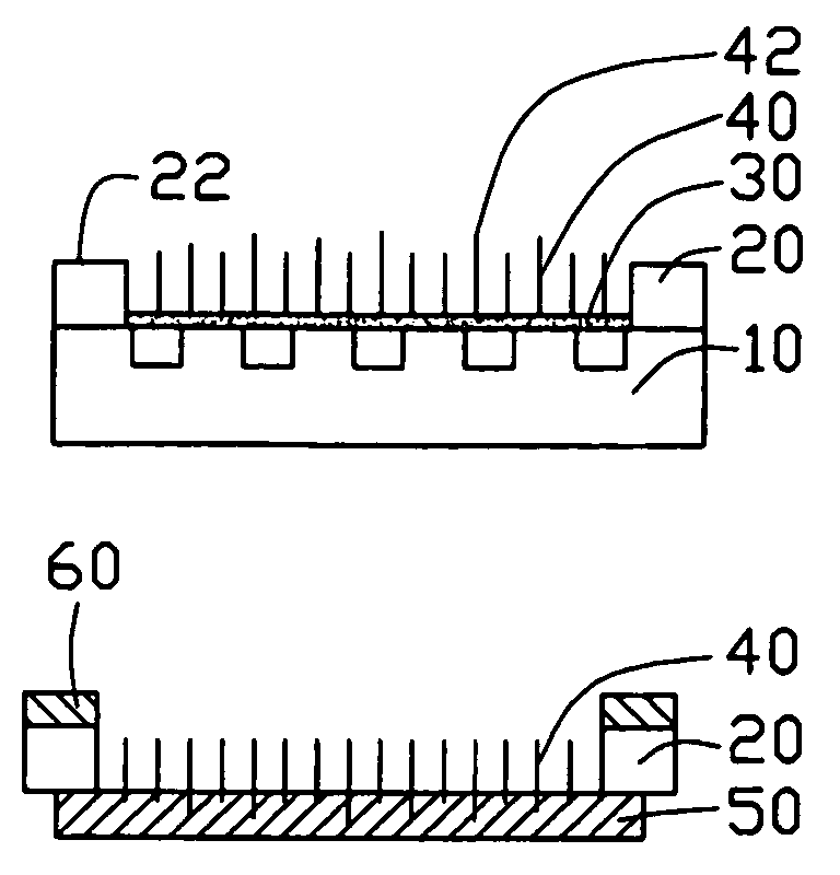
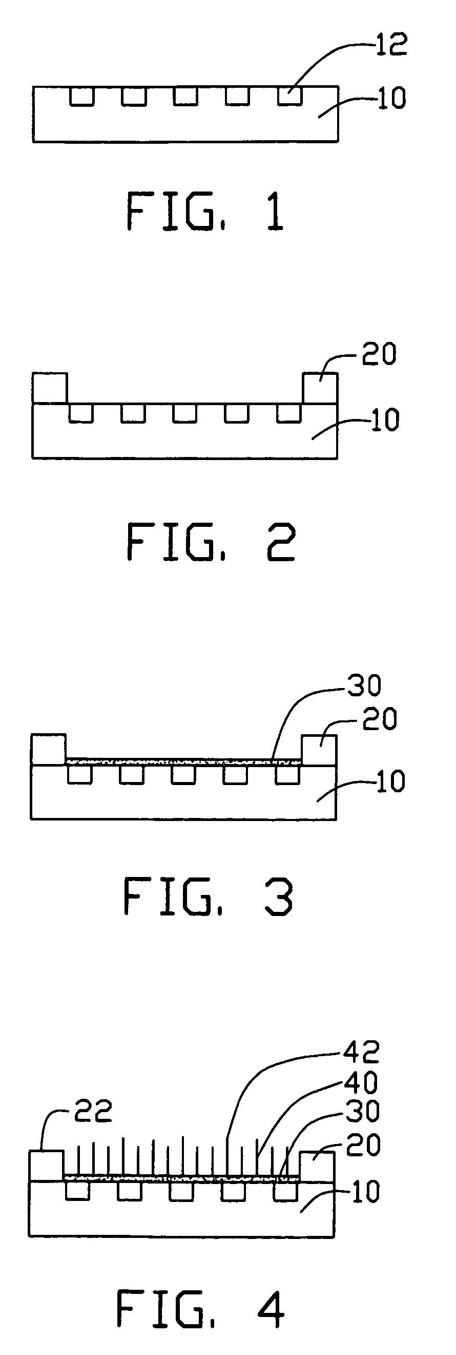
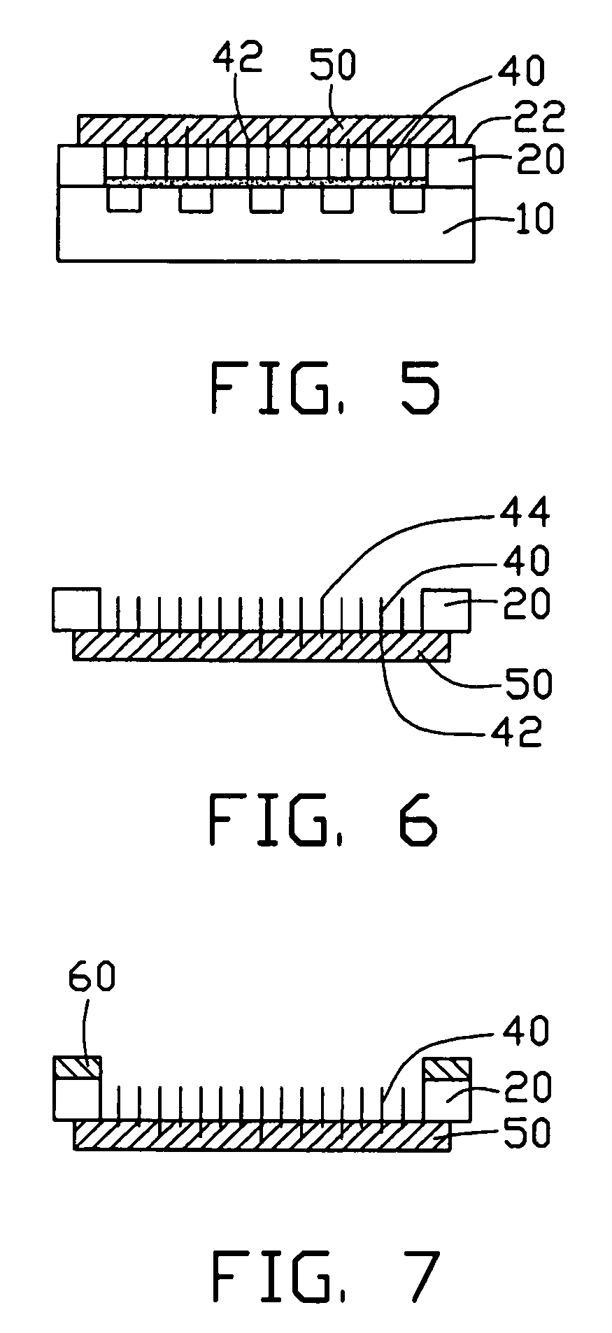
[0020]Referring initially to FIG. 7, a carbon nanotube-based field emission device in accordance with a preferred embodiment of the present invention comprises: a cathode electrode 50, a carbon nanotube array 40 formed substantially perpendicularly to the cathode electrode 50, and gate electrodes 60 formed on an insulative barrier 20 adjacent the carbon nanotube array 40. The barrier 20 is positioned on the cathode electrode 50, and insulates the gate electrodes 60 from the cathode electrode 50. The carbon nanotube array 40 comprises a plurality of carbon nanotubes (not labeled). Preferably, each carbon nanotube has an open tip to facilitate electron emission therefrom. Referring also to FIG. 6, the carbon nanotube array 40 defines a growth end 42, and a root end 44 opposite to the growth end 42. The growth end 42 is embedded in and thus is in electrical contact wit...


PUM

PropertyMeasurementUnit
flatnessaaaaaaaaaa
heightaaaaaaaaaa
heightaaaaaaaaaa

Abstract

A carbon nanotube-based field emission device in accordance with the invention includes: a cathode electrode (50), a carbon nanotube array (40) formed perpendicularly on the cathode electrode, a barrier (20) and a gate electrode (60). The carbon nanotube array has a growth end (42) electrically contacting with the cathode electrode, and an opposite root end (44) for emitting electrons therefrom. The root end of the carbon nanotube array defines a substantially planar surface having a flatness of less than 1 micron.

Description

BACKGROUND OF THE INVENTION[0001]1. Field of the Invention[0002]The present invention relates to a field emission device, and more particularly to a field emission device utilizing carbon nanotubes as emitters.[0003]2. Description of Prior Art[0004]Carbon nanotubes are a novel carbonaceous material discovered by Iijima, a researcher of NEC corporation, in 1991. Relevant information was reported in an article by Iijima, entitled “Helical Microtubules of Graphitic Carbon” (Nature, Vol.354, P56, 1991). Carbon nanotubes can transmit an extremely high electrical current and can emit electrons at a very low voltage of less than 100 volts, which makes it a very promising material for field emission applications. Walt A. de Heer et al. reported a field emission device employing carbon nanotubes as an electron emission source in an article entitled “A Carbon Nanotube Field-Emission Electron Source” (Science, Vol. 270, P1179-1180, 1995). Shoushan Fan et al. reported a method using a CVD (chem...

Claims


Application Information

Patent Timeline
Patent Type & Authority Patents(United States)
IPC IPC(8): H01J1/02H01J1/304H01J9/02
CPCB82Y10/00H01J1/3044H01J9/025H01J2201/30469
Inventor LIU, LIANGFAN, SHOUSHAN
Owner TSINGHUA UNIV
Why Eureka
Try Eureka