Method For Manufacturing Thin-Film Transistor Substrate And Thin-Film Transistor Substrate Manufactured With Same

a thin-film transistor and substrate technology, applied in the field of liquid crystal display, can solve the problems of increasing the manufacturing cost, and reducing the yield rate, so as to improve the yield rate, improve the stability and uniformity of the thin-film transistor substrate, and expand the likelihood of mass production

Inactive Publication Date: 2015-05-14
SHENZHEN CHINA STAR OPTOELECTRONICS TECH CO LTD
View PDF3 Cites 5 Cited by
  • Summary
  • Abstract
  • Description
  • Claims
  • Application Information

AI Technical Summary

Benefits of technology

[0007]An object of the present invention is to provide a method for manufacturing a thin-film transistor substrate, which can effective avoid damages of an oxide semiconductor layer caused by etching processes of metal signal lines and source / drain electrodes, enhance stability and uniformity of thin-film transistor substrates, improve yield rate, expand the likelihood of mass production of oxide semiconductor thin-film transistor substrate, and can reduce one round of photolithographic process to thereby greatly lower down the manufacture cost and improve manufacture yield rate.

Problems solved by technology

Using a dry etching process instead, however, causes problems of poor uniformity of etching.
However, forming the additional etch-stop layer requires an additional photolithographic process.
The photolithographic process comprises various operations, such as film forming, exposure, development, etching, and peeling, so that forming such an additional etch-stop layer would greatly increase the manufacture cost and lower down yield rate.

Method used


Image

  • Method For Manufacturing Thin-Film Transistor Substrate And Thin-Film Transistor Substrate Manufactured With Same
  • Method For Manufacturing Thin-Film Transistor Substrate And Thin-Film Transistor Substrate Manufactured With Same
  • Method For Manufacturing Thin-Film Transistor Substrate And Thin-Film Transistor Substrate Manufactured With Same

Examples


Embodiment Construction

[0055]To further expound the technical solution adopted in the present invention and the advantages thereof, a detailed description is given to a preferred embodiment of the present invention and the attached drawings.

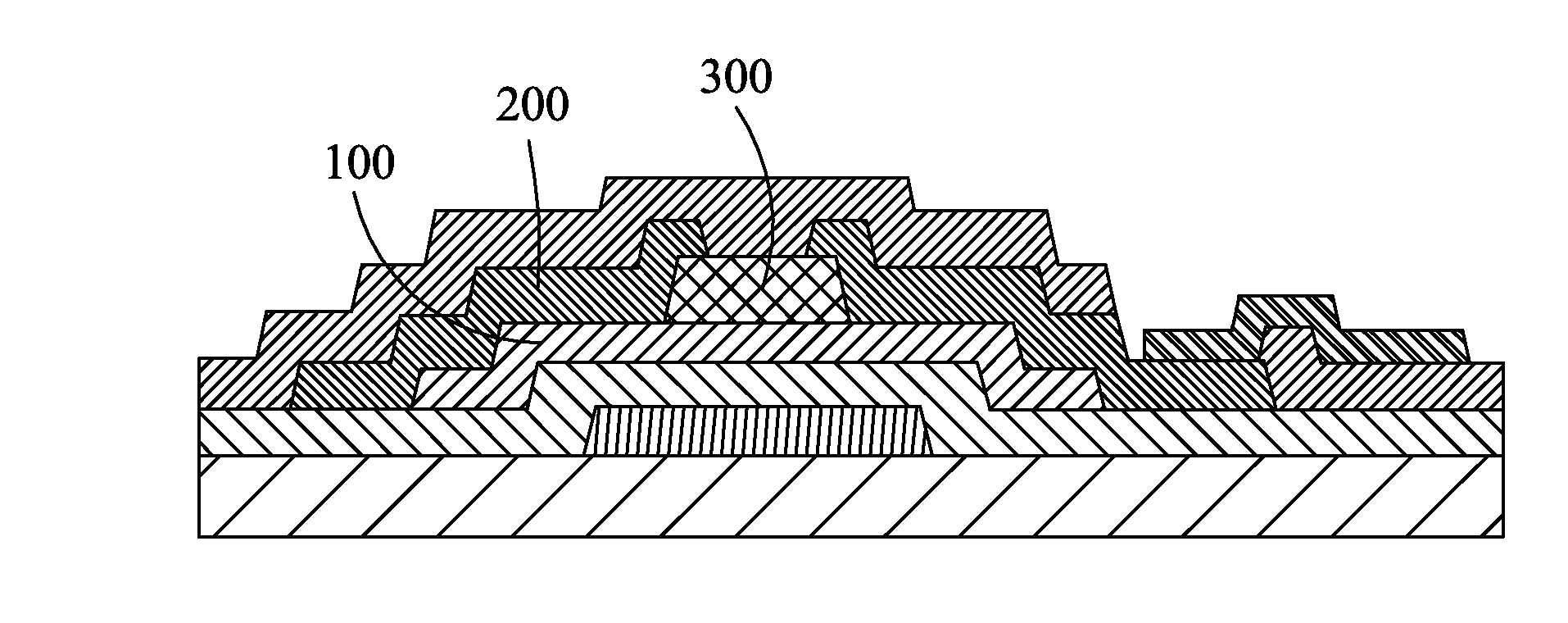
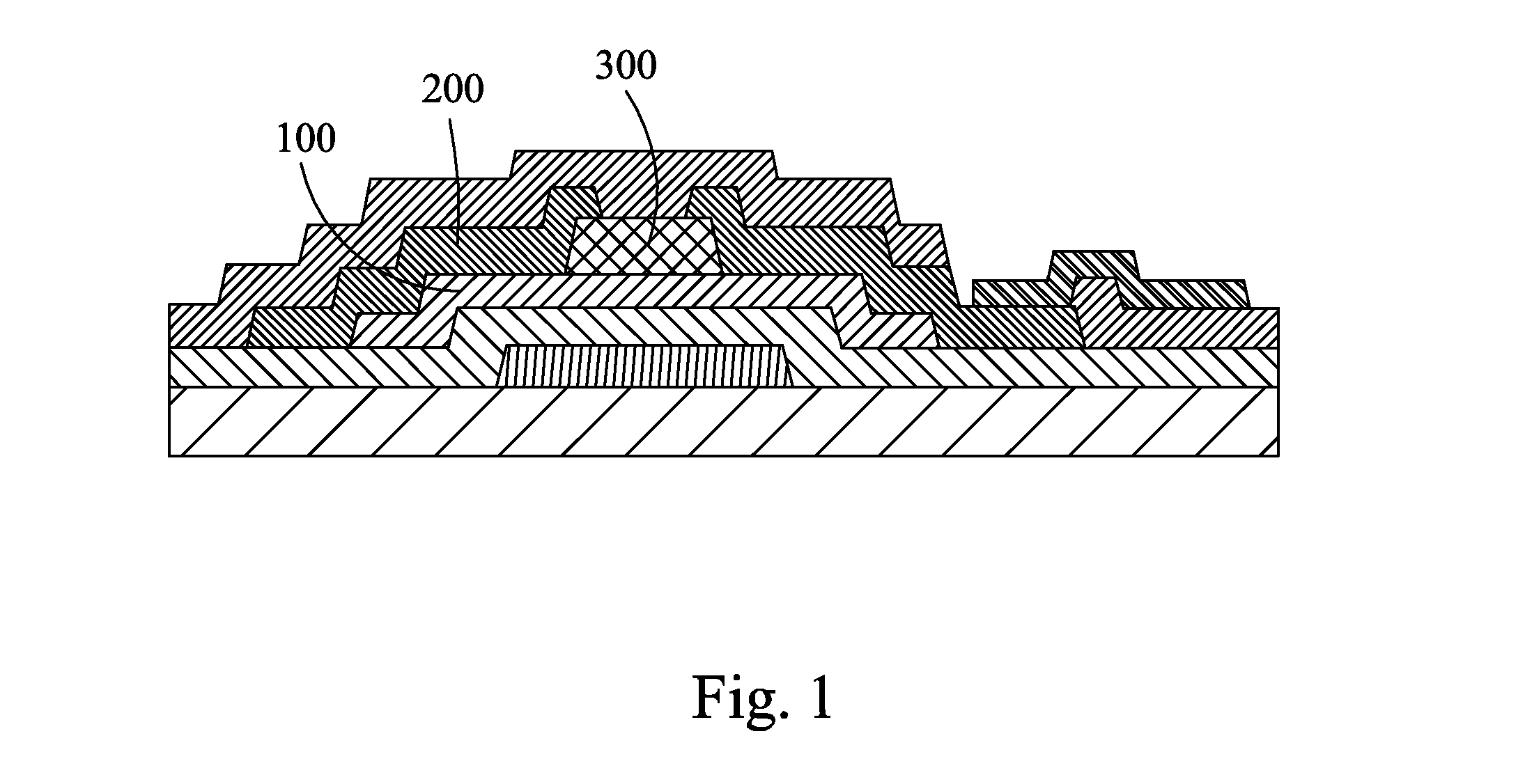
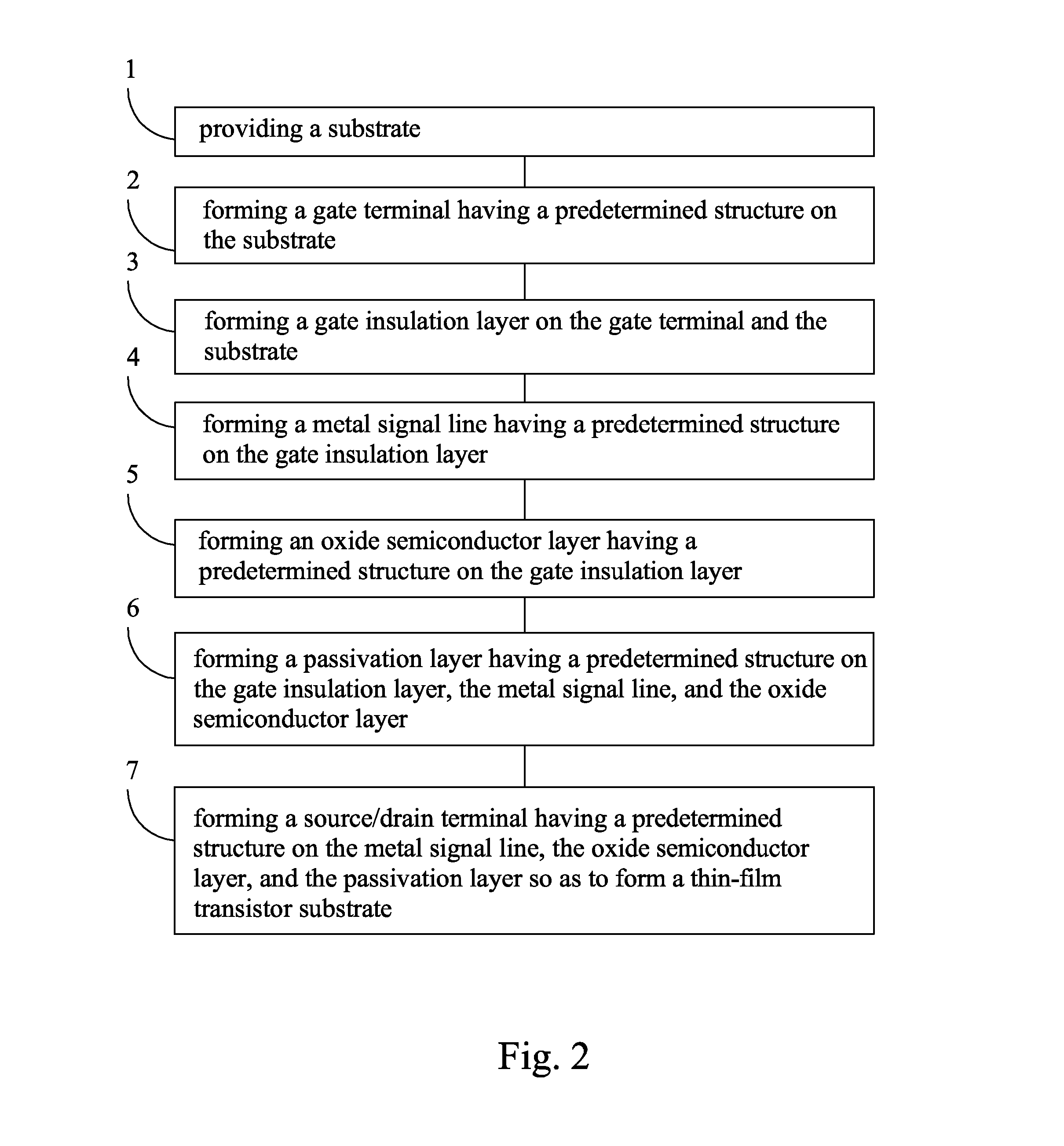
[0056]Referring to FIG. 2, with additional reference had to FIGS. 3-8, the present invention provides a method for manufacturing a thin-film transistor substrate, which comprises the following steps:

[0057]Step 1: providing a substrate 20.

[0058]The substrate 20 is a transparent substrate, preferably a glass substrate or a plastic substrate. In the instant embodiment, the substrate 20 is a glass substrate.

[0059]Step 2: forming a gate terminal 22 having a predetermined structure on the substrate 20.

[0060]A first-round photolithographic process is applied to form the gate terminal 22 having the predetermined structure on the substrate 20 and the specific processing flow includes: first depositing a first metal layer on the substrate 20 and then applying a mask or a halfton...


PUM


Abstract

The present invention provides a method for manufacturing a thin-film transistor substrate and a thin-film transistor substrate manufactured with the method. The method includes: (1) providing a substrate (20); (2) forming a gate terminal (22) having a predetermined structure on the substrate (20); (3) forming a gate insulation layer (24) on the gate terminal (22) and the substrate (20); (4) forming a metal signal line (26) having a predetermined structure on the gate insulation layer (24); (5) forming an oxide semiconductor layer (28) having a predetermined structure on the gate insulation layer (24); (6) forming a passivation layer (32) having a predetermined structure on the gate insulation layer (24), the metal signal line (26), and the oxide semiconductor layer (28); and (7) forming a source/drain terminal (34) having a predetermined structure on the metal signal line (26), the oxide semiconductor layer (28), and the passivation layer (32) so as to form a thin-film transistor substrate.

Description

BACKGROUND OF THE INVENTION[0001]1. Field of the Invention[0002]The present invention relates to the field of liquid crystal displaying, and in particular to a method for manufacturing a thin-film transistor (TFT) substrate and a thin-film transistor substrate manufactured with the method.[0003]2. The Related Arts[0004]A thin-film transistor (TFT) has been widely used in electronic devices to serve as a switching device and a driving device. Specifically, the thin-film transistors can be formed on a glass substrate or a plastic substrate so that they are commonly used in the field of flat panel display devices, such as a liquid crystal display (LCD), an organic light-emitting display (OLED), and an electro-phoretic display (EPD).[0005]Oxide semiconductors have a relatively high electron mobility (the electron mobility of oxide semiconductors >10 cm2 / Vs, while the mobility of a-Si being only 0.5-0.8 cm2 / Vs) and, compared to low temperature poly-silicon (LTPS), the oxide semiconduc...

Claims


Application Information

Patent Timeline
Patent Type & Authority Applications(United States)
IPC IPC(8): H01L27/12H01L21/441H01L29/45H01L21/02H01L29/786H01L29/66
CPCH01L27/1225H01L27/1259H01L29/78603H01L29/7869H01L21/441H01L29/45H01L21/02565H01L21/02422H01L29/66969H01L21/02488H01L27/124H01L27/1248
Inventor LI, WENHUITSENG, CHIHYUAN
Owner SHENZHEN CHINA STAR OPTOELECTRONICS TECH CO LTD
Why Eureka
Try Eureka