
Semiconductor device and its manufacturing method

a semiconductor chip and manufacturing method technology, applied in semiconductor devices, semiconductor/solid-state device details, electrical apparatus, etc., can solve the problems of increasing complexity, circuit configuration becoming more and more complicated and diversified, and difficulty in ensuring a space for arranging a plurality of leads in connecting portions of semiconductor chips, etc., to reduce the time required for testing, simplify the testing, and easy and surely trim the leads

Inactive Publication Date: 2008-01-22
PS4 LUXCO SARL
View PDF17 Cites 0 Cited by
  • Summary
  • Abstract
  • Description
  • Claims
  • Application Information

AI Technical Summary

Benefits of technology

This approach simplifies testing, reduces testing time, and ensures efficient use of substrates by allowing the same lead patterns to be used across layers, effectively coping with increased signal demands and preventing substrate shortages.

Problems solved by technology

However, since scaling down of the semiconductor chip has been advanced in recent years, it is in many cases difficult to ensure a space for arranging a plurality of leads in connecting portions of the semiconductor chip.
With the capacity increase owing to the further scaling down of the semiconductor device, circuit configuration becomes more and more complicated and diversified.
Therefore, the testing becomes complicated and the time required for the testing is increased.

Method used


Image

  • Semiconductor device and its manufacturing method
  • Semiconductor device and its manufacturing method
  • Semiconductor device and its manufacturing method

Examples


first embodiment

[0066](First Embodiment)

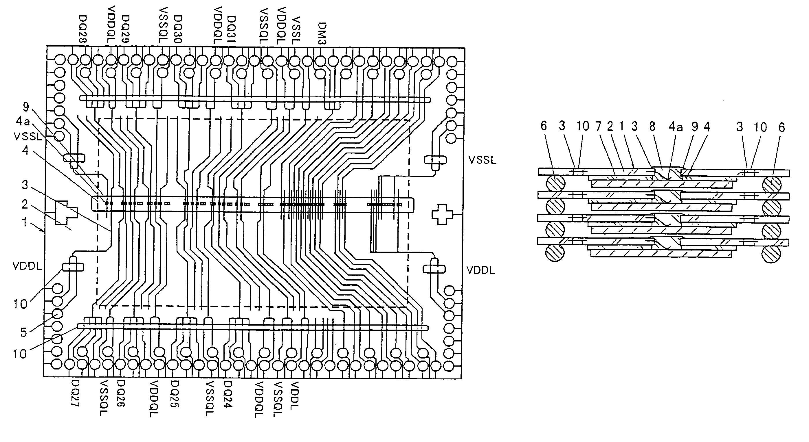
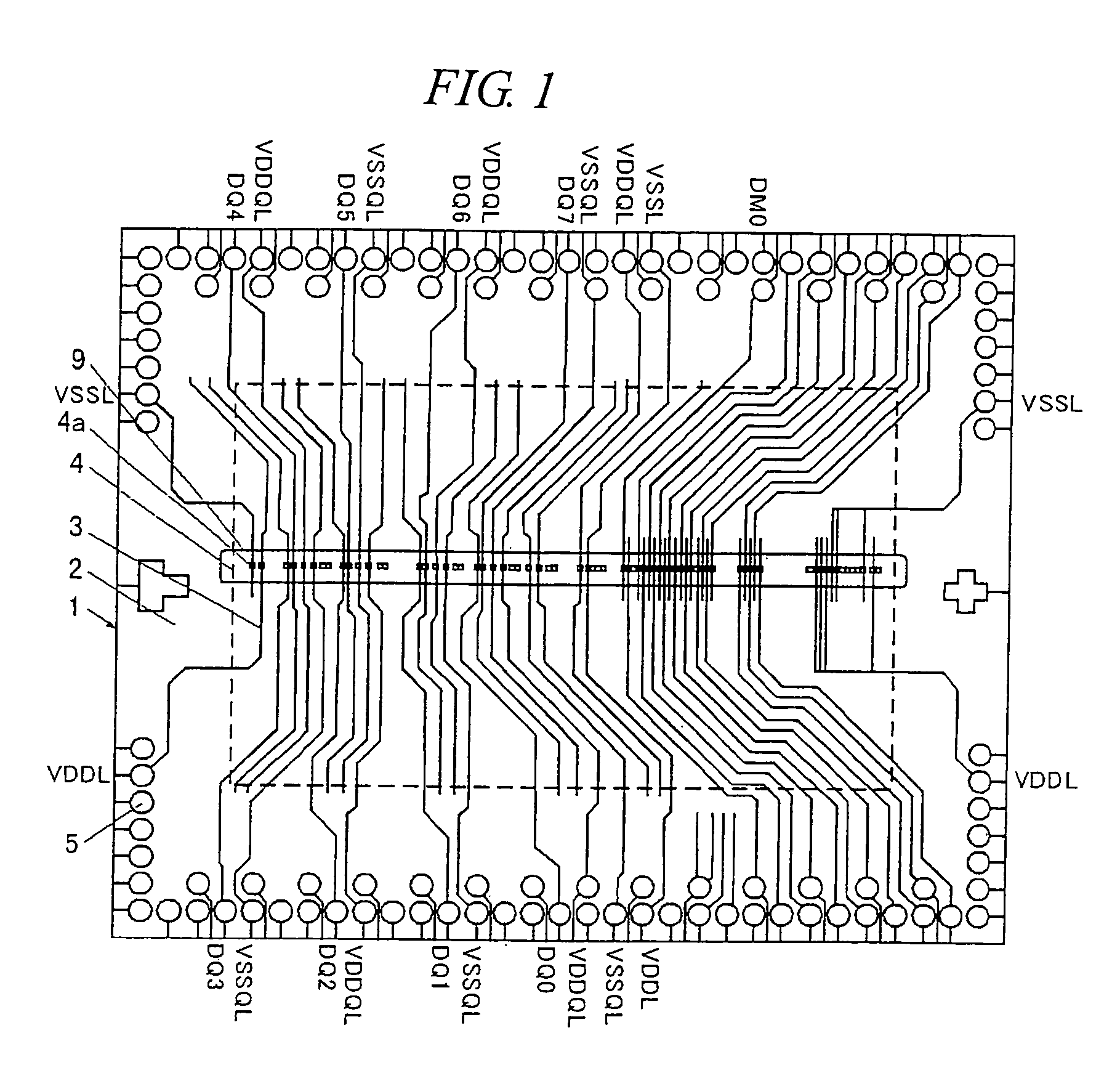
[0067]FIG. 6 is a plan view showing a state of mounting semiconductor chips on tape carrier substrates used in a semiconductor device according to an embodiment of the present invention.

[0068]A tape carrier substrate 1 is composed of a film-shaped insulating substrate 2 made of polyimide etc. on which leads 3 each made of a metal film (hereinafter “lead”) are formed. One end of each lead 3 is connected to a bonding pad 4a (hereinafter ‘pad’) of a semiconductor chip 4 and the other end thereof is connected to a connection terminal 5 of the tape carrier substrate 1. The respective tape carrier substrates are connected by bump electrodes 6 formed on the connection terminals 5. The semiconductor chip 4 is fixed to the tape carrier substrate 1 by an adhesive layer 7, and a connecting portion between the lead 3 and the pad 4a is covered with an encapsulation material 8 such as a resin.

[0069]This tape carrier substrate is used for the center-pad type semiconductor c...

second embodiment

[0100](Second Embodiment)

[0101]FIG. 33 is a plan view showing a structure before trimming of leads, in a state of mounting the semiconductor chip on the tape carrier substrate used in a semiconductor device according to another embodiment of the present invention. FIG. 34 is a longitudinal sectional view showing a state of mounting semiconductor chips and stacking tape carrier substrates after trimming of leads. The tape carrier substrate of this embodiment is different from that of the first embodiment in that this embodiment is used for the corner-pad type semiconductor chip 4, at the peripheral portions of which the bonding pads 4a (hereinafter “pad”) are disposed.

[0102]The tape carrier substrate 1 is composed of a film-shaped insulating substrate 2 made of polyimide etc. on which leads 3 each made of a metal film (hereinafter “lead”) are formed. One ends of the leads 3 are connected to the pads 4a of the semiconductor chip 4 and the other ends thereof are connected to the connec...


PUM


Abstract

In a semiconductor device in which a plurality of substrates each mounting a semiconductor chip are stacked, one ends of the leads formed on the substrates are connected to the semiconductor chip and the other ends thereof are connected to connection terminals of the substrates. At least one of the leads are branched into two or more in the vicinity of the connection terminals, and one ends of the branched leads are connected to the connection terminals. A technique for sorting good products is performed in a state in which the chips are mounted on the substrates.

Description

CROSS-REFERENCE TO RELATED APPLICATION[0001]The present application claims priority from Japanese patent application No. JP 2003-303974 filed on Aug. 28, 2003, the content of which is hereby incorporated by reference into this application.BACKGROUND OF THE INVENTION[0002]The present invention relates to a semiconductor device and its manufacturing method. More particularly, the present invention relates to a technique effectively applied to a semiconductor device in which substrates each mounting a semiconductor chip are stacked.[0003]In the manufacture of a semiconductor device, semiconductor elements or line patterns are collectively formed in a plurality of element forming regions provided in a wafer made of single crystal silicon etc. so as to form a predetermined circuit; and the wafer is trimmed along a scribing region between the adjacent element forming regions and there is performed dicing by which the respective element forming regions are separated as individual semicondu...

Claims


Application Information

Patent Timeline
Patent Type & Authority Patents(United States)
IPC IPC(8): H01L23/48H01L23/52H01L25/18H01L23/31H01L23/495H01L23/538H01L25/10H01L25/11
CPCH01L23/3128H01L23/49572H01L25/105H01L24/50H01L23/5382H01L2924/15311H01L2924/3511H01L2225/1023H01L2225/1058H01L2924/15331H01L24/86H01L2924/12042H01L2924/00
Inventor KAGAYA, YUTAKAKUSANAGI, KEIYOKIKUCHI, KOYAHATASAWA, AKIHIKO
Owner PS4 LUXCO SARL
Features
  • Generate Ideas
  • Intellectual Property
  • Life Sciences
  • Materials
  • Tech Scout
  • Unparalleled Data Quality
  • Higher Quality Content
  • 60% Fewer Hallucinations
Learn More