
Optical device

a technology of optical devices and optical fibers, applied in the field of optical fiber arrays, can solve the problems of low yield, excessive stress, reliability problems, etc., and achieve the effect of increasing the reliability of a monitoring function and increasing the yield

Inactive Publication Date: 2008-01-22
NGK INSULATORS LTD
View PDF96 Cites 3 Cited by
  • Summary
  • Abstract
  • Description
  • Claims
  • Application Information

AI Technical Summary

Benefits of technology

The present invention provides an optical device with improved monitoring function and increased yield. The device includes a slit for dividing signal light, a filter member, and a gel material filling the slit. The gel material has low stress and low refractive index, which reduces thermal variations and improves the monitoring function. The refractive index of the gel material matches that of the light transmitting means to prevent etalon effect. The gel material can be made of silicone-based material with low humidity retaining ability and low refractive index change due to humidity. The optical device can also include an optical element and a slit with specific width and angle ranges for improved performance.

Problems solved by technology

If the optical fiber splicing resin is used as the resin that fills the parallel groove, then since the parallel groove which has a width of about several tens μm is filled with the hard resin having such a large Young's modulus, excessive stresses are developed, tending to give rise to a reliability problem, for example.
If the refractive index matching material is used as the resin that fills the parallel groove, then since the refractive index matching material is generally in a low-viscosity liquid phase, it is difficult to keep the refractive index matching material filled in the parallel groove, tending to result in a low yield.

Method used


Image

  • Optical device
  • Optical device
  • Optical device

Examples


Embodiment Construction

[0028]An embodiment in which an optical device according to the present invention is applied to a 4 channel in-line power monitor module, for example, will be described below with reference to FIGS. 1 through 3.

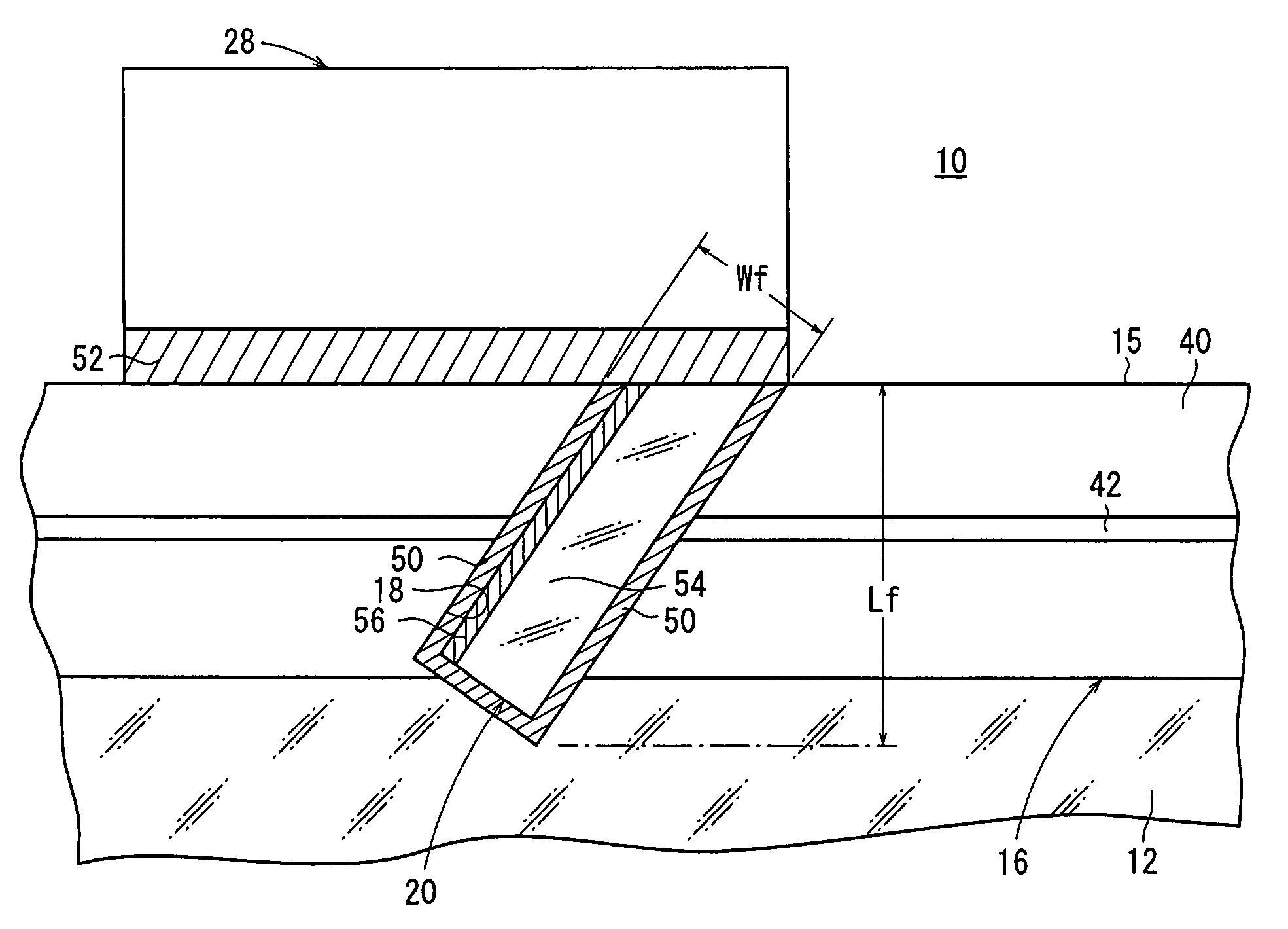
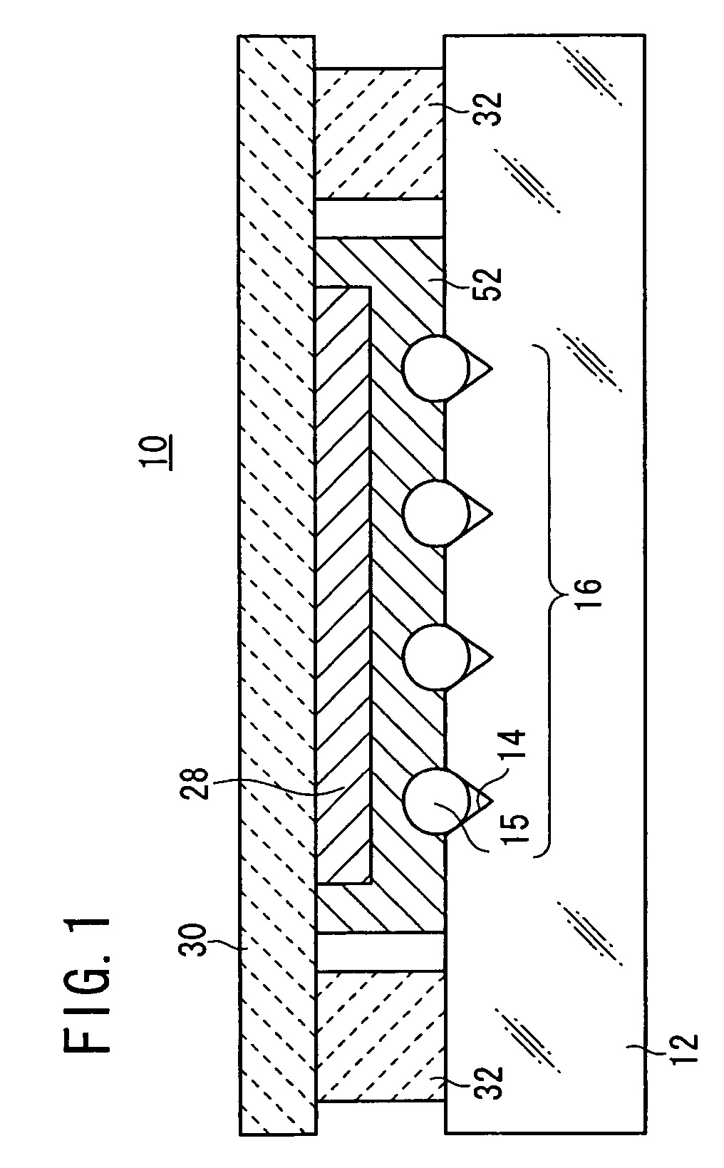
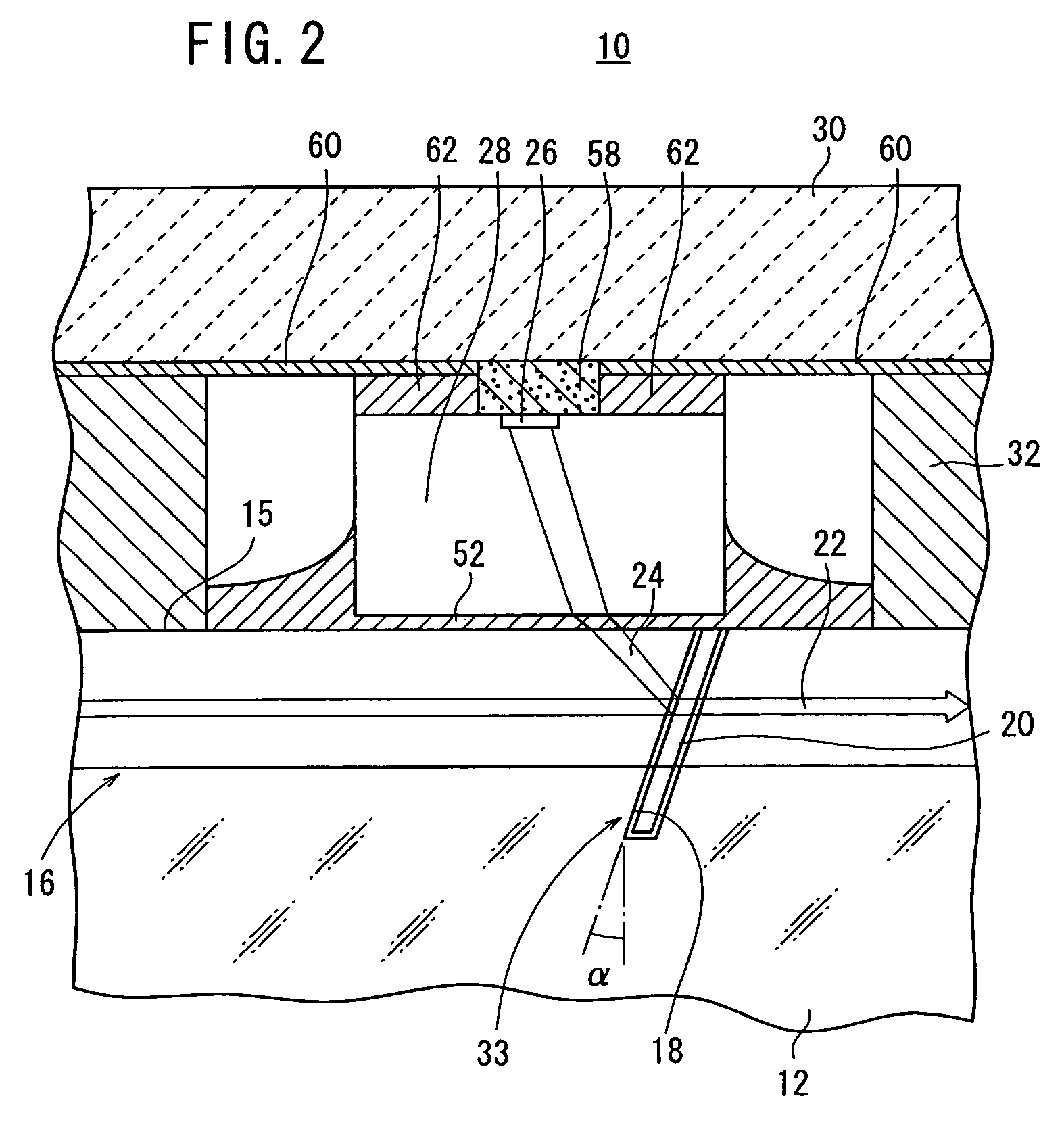
[0029]As shown in FIG. 1, an optical device 10 according to an embodiment of the present invention has a glass substrate 12, an optical fiber array 16 comprising a plurality of optical fibers 15 fixed in a plurality of V-shaped grooves 14 defined in the glass substrate 12. As shown in FIG. 2, a slit 18 extends from respective upper surfaces of the optical fibers 15 into the glass substrate 12 with a filter member 20 inserted in the slit 18 with a PD(PhotoDiode) array 28, having a plurality of active layers 26 for detecting light (divided light) 24 divided by at least the filter member 20, for detecting signal light 22 passing through the optical fibers 15, and a submount 30 fixing the PD array 28 so as to face the optical fiber array 16, and a spacer 32 for stably fixing at l...


PUM


Abstract

An optical device includes an optical fiber having a core and a cladding, a slit extending from the upper surface of the optical fiber into a glass substrate, a filter member inserted in the slit, and a PD array for detecting divided light. A first high-polymer gel material fills a gap between the slit and a filter member within the slit. A second high-polymer gel material is interposed between an optical fiber array and the PD array and disposed on an optical path of the light divided by the filter member.

Description

CROSS REFERENCE TO RELATED APPLICATIONS[0001]This application is a continuation-in-part of International Application No. PCT / JP2003 / 016348, having an international filing date of Dec. 19, 2003, which designated. the United States, and is a continuation-in-part application of U.S. application Ser. No. 10 / 732,203, filed Dec. 10, 2003 now abandoned, which claims the benefit under 35 USC §119(e) of U.S. Provisional Application Ser. No. 60 / 435,105, filed Dec. 20, 2002, the entireties of which are incorporated herein by reference.BACKGROUND OF THE INVENTION[0002]1. Field of the Invention[0003]The present invention relates to an optical fiber array having one or more optical fibers or an optical device having one or more optical waveguides, and more particularly to an optical device suitable for monitoring signal light while it is being propagated through such optical transmitting means.[0004]2. Description of the Related Art[0005]For the present optical communication technology, it is imp...

Claims


Application Information

Patent Timeline
Patent Type & Authority Patents(United States)
IPC IPC(8): G02B6/12G02B6/34G02B6/42
CPCG02B6/4214G02B6/4249G02B6/2793G02B6/4239G02B6/4295
Inventor FUKUYAMA, MASASHIIWASAKI, YASUNORIIDE, AKIYOSHI
Owner NGK INSULATORS LTD
Learn More