Solid image pickup device, image pickup system and method of driving solid image pickup device

a pickup device and solid image technology, applied in the field of image pickup systems and methods of driving solid image pickup devices, can solve the problems of afterimage and noise, depleting voltage, and charge quantity qsat, and achieve the effect of less noise and smaller power consumption

Inactive Publication Date: 2008-01-29
CANON KK
View PDF18 Cites 123 Cited by
  • Summary
  • Abstract
  • Description
  • Claims
  • Application Information

AI Technical Summary

Benefits of technology

[0023]It is one object of the present invention to provide a solid image pickup device having a less amount of noise at a smaller power consumption in comparison with a conventional one, a method of driving the solid image pickup system, and an image pickup system.

Problems solved by technology

The residual electrons of this time causes an afterimage and a noise.
The saturated charge quantity Qsat, or the depleting voltage, has a problem, however, likely to be affected by the production process.
As a result, the yield of production lowers.
As well known, a high power source voltage brings about a rise in power consumption.
This results in the deterioration of performances of an APS chip.

Method used


Image

  • Solid image pickup device, image pickup system and method of driving solid image pickup device
  • Solid image pickup device, image pickup system and method of driving solid image pickup device
  • Solid image pickup device, image pickup system and method of driving solid image pickup device

Examples


embodiment 1

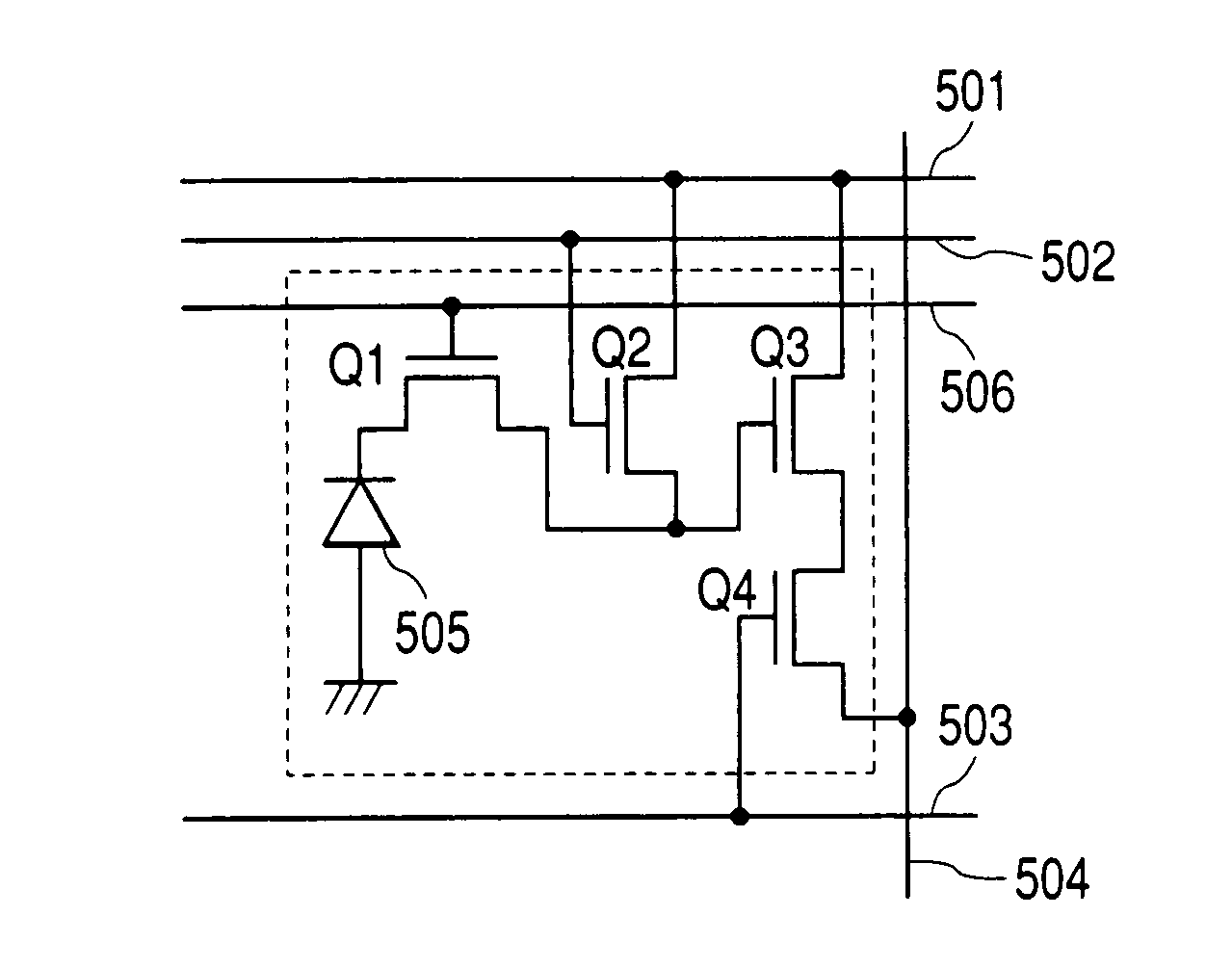
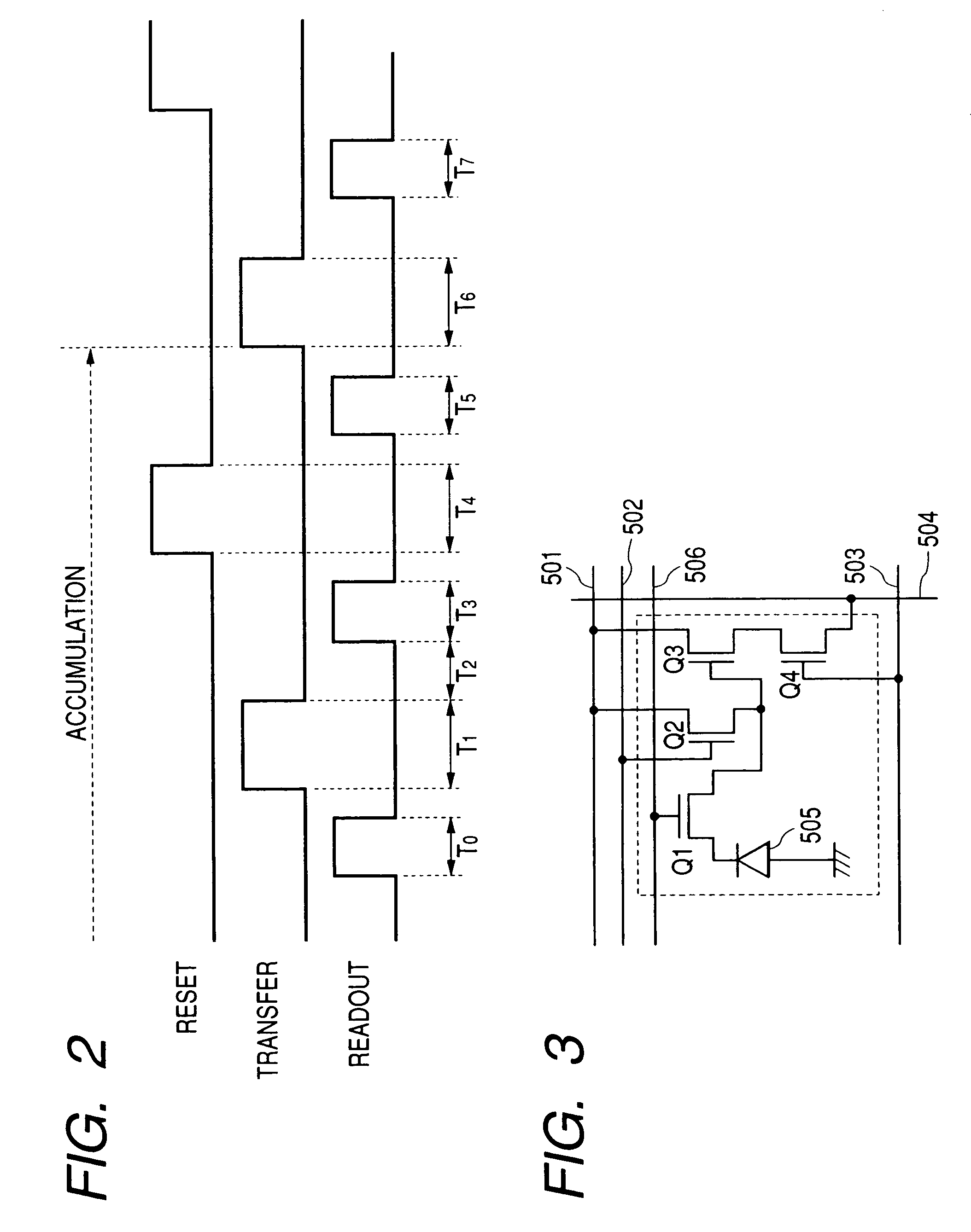
[0093]The equivalent circuit diagram of the pixel used in this embodiment is the same as that shown in FIG. 3, and in this embodiment this pixel is arranged in two-dimensions to form an area sensor.

[0094]In FIG. 3, Numeral 505 denotes an embedded-type photodiode corresponding to the photoelectric conversion part. As an embedded-type photodiode in this embodiment, an n-type accumulative layer for accumulating photo-electric charges and a P+-type layer comprising a p-type semiconductor of a high impurity for suppressing the surface dark current between this n-type layer and an insulating layer thereon were provided in a well comprising a p-type semiconductor formed in the substrate to form an embedded-type photodiode as shown in FIG. 1. The depleting voltage of this photodiode is 1.0 volt.

[0095]An nMOS transistor was used for an input transistor of a source follower amplifier as the signal amplifying means Q3, and the nMOS transistor was used for selecting a reading out row as a selec...

embodiment 2

[0119]The physical configuration of individual pixels and the circuitry of a solid image pickup device according to Embodiment 2 are the same as those Embodiment 1.

[0120]Difference from Embodiment 1 lies in using the circuit shown in FIG. 6 as a readout circuit.

[0121]FIG. 6 is a schematic circuit diagram of a readout circuit with addition means, used in the present invention.

[0122]Output of each pixel is read out by the output signal retention means 702 connected to a signal output line 704. For output signal retention means 702 for once retaining an output signal, specifically, a plurality of capacity elements can be used. In case of this embodiment, the switch S1 in FIG. 5 turns ON / OFF at the primary (first) readout to retain a noise signal and an output signal in a capacity. At the second readout, the switch S2 turns ON / OFF to retain a noise signal and an output signal in another capacity, and at the final (third) readout, the switch S3 turns ON / OFF to retain a noise signal and a...

embodiment 3

[0133]FIG. 8 is a circuit diagram of one pixel and a readout circuit according to the present invention.

[0134]Numerals 901 and 901′ denote power supply lines for applying the reset voltage and the power supply voltage of an amplification transistor. Numerals 902 and 902′ denote reset switch lines for controlling the operation of the reset switches Q2 and Q2′. Numeral 904 denotes a signal output line. Numeral 905 denotes a photodiode. Numerals 906 and 906′ denote transfer switch lines for controlling the operation of transfer switches Q1 and Q1′, respectively.

[0135]In Embodiments 1 and 2, one source follower was disposed for each pixel and the input part of a source follower was reset in the time series for every readout.

[0136]In this embodiment, two source followers Q3 and Q3′ are disposed for each pixel. Here, the input parts of source followers Q3 and Q3′ are simultaneously reset by turning the reset switches Q2 and Q2′ to ON.

[0137]Thereafter, the selective switch Q4, the noise sw...


PUM


Abstract

The solid image pickup device of the present invention comprises a photoelectric conversion part, a charge-voltage conversion part for converting electric charges from the photoelectric conversion part to voltage signals, a signal amplifier for amplifying the voltage signals generated in the charge-voltage conversion part, charge transfer means for transferring photo-electric charges from the photoelectric conversion part to the charge-voltage conversion part, and means for applying a certain voltage to a charge-voltage conversion part, wherein at least two readout operations for reading out the photo-electric charges accumulated during a period of accumulating photo-electric charges in the photoelectric conversion part via a signal amplifier.

Description

BACKGROUND OF THE INVENTION[0001]1. Field of the Invention[0002]The present invention relates to a solid image pickup device, an image pickup system and a method of driving the solid image pickup device. In particular, the present invention relates to a solid image pickup device comprising a photoelectric conversion part, a charge-voltage conversion part for converting electric charges from the photoelectric conversion part to voltage signals, signal amplification means for amplifying the voltage signals, charge transfer means for transferring photo-electric charges from the photoelectric conversion part to the charge-voltage conversion part, and means for inputting a certain voltage to the charge-voltage conversion part; an image pickup system; and a method of driving the solid image device.[0003]2. Related Background Art[0004]As representatives of solid image pickup devices, there is a device comprising a photodiode and a CCD shift register, and a device called APS (Active Pixel S...

Claims


Application Information

Patent Timeline
Patent Type & Authority Patents(United States)
IPC IPC(8): H04N3/14H04N5/335
CPCH04N5/355H04N5/35527H04N5/35572H04N5/3597H04N5/37452H04N5/37457H04N25/575H04N25/57H04N25/587H04N25/589H04N25/626H04N25/778H04N25/771
Inventor KOIZUMI, TORU
Owner CANON KK
Why Eureka
Try Eureka