Stacked die package

a technology of stacked dies and dies, applied in the direction of semiconductor devices, semiconductor/solid-state device details, electrical devices, etc., can solve the problems of high cost, limited number of functions realizable on a single chip, and more complex functions to be realized

Inactive Publication Date: 2008-02-05
POLARIS INNOVATIONS LTD
View PDF9 Cites 60 Cited by
  • Summary
  • Abstract
  • Description
  • Claims
  • Application Information

AI Technical Summary

Benefits of technology

[0014]In another aspect, the invention increases the reliability of a stacked die package by decreasing the number of interfaces within the package.
[0015]In a further aspect, the invention decreases the total height of the package or increases the number of chips in the package with maintaining the total package height.
[0016]According to an embodiment of the invention, the bottom die can be modified in advance to die bonding to provide additional area around the silicon edge. That way the use of a spacer is not needed. The bottom die is embedded in a polymer material by molding (reconstitution) resulting in a frame around the die. This frame is a fan-out area, the chip area is now larger than the bare silicon of the die. The redistribution line that is used to distribute connections from the pads on the chip to the edges of the die package can be elongated to the edge of the frame. The position for the bond wire interconnect is transferred to the edge of the frame as well. That way the bottom die on the substrate is provided with a larger area than a next die, which can be die bonded with an adhesive at the top side of the first reconstituted die. The area out of the die shadow of the upper die can now used to connect the first die with the substrate or the bottom die by wire bonding.
[0017]The result is that a spacer is no longer necessary, all process steps, necessary for assembling the spacer can be left out. This leads to lower packaging costs and less reliability issues due to a reduced number of material interfaces.
[0018]Another feature of the invention is that more dies can be stacked at a given total height, or the total package height of two stacked dies can be reduced.

Problems solved by technology

The development of the application of integrated circuits shows that more complex functions are to be realized but there are limitations of the number of functions realizable on a single chip.
It seems to be clear that this is a very expensive technology (serial processes with high accuracy), even in case that more than two dies are stacked.
The high number of interfaces (due to the spacer) results in a lower processing yield.
The problem of this prior art is that the dies must be equal in size but it is possible to stack very thin dies.

Method used


Image

  • Stacked die package
  • Stacked die package
  • Stacked die package

Examples


Embodiment Construction

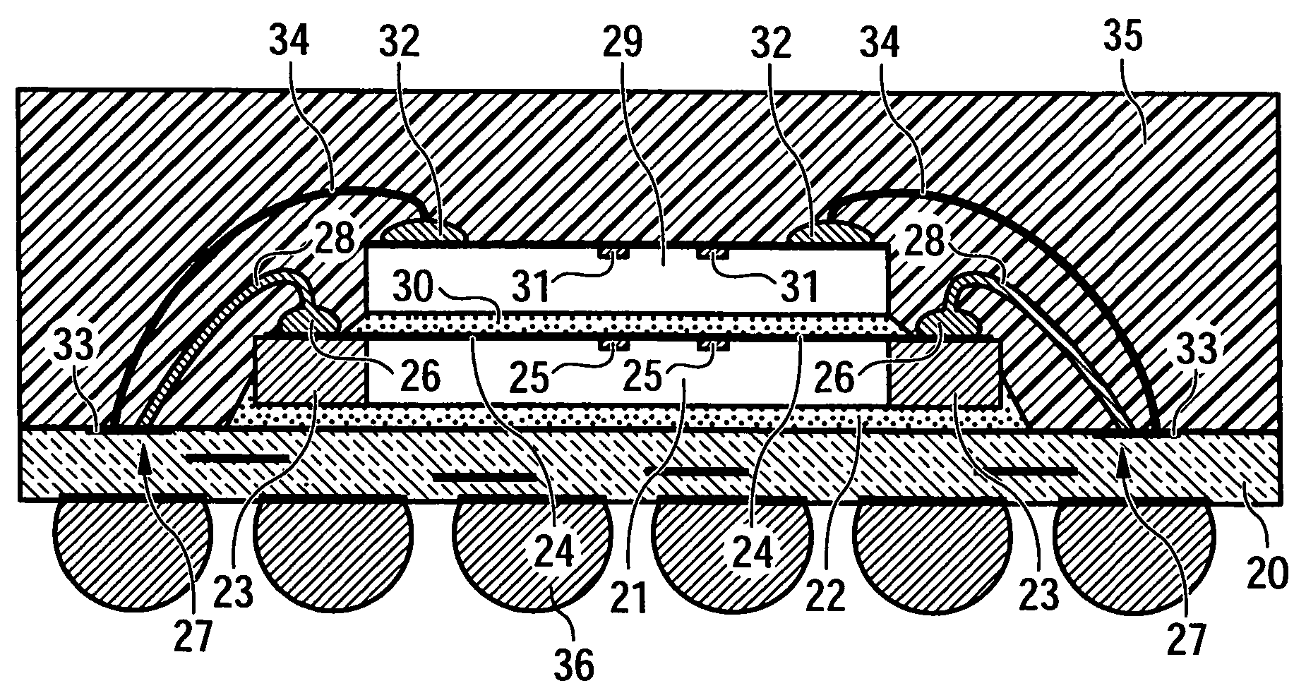
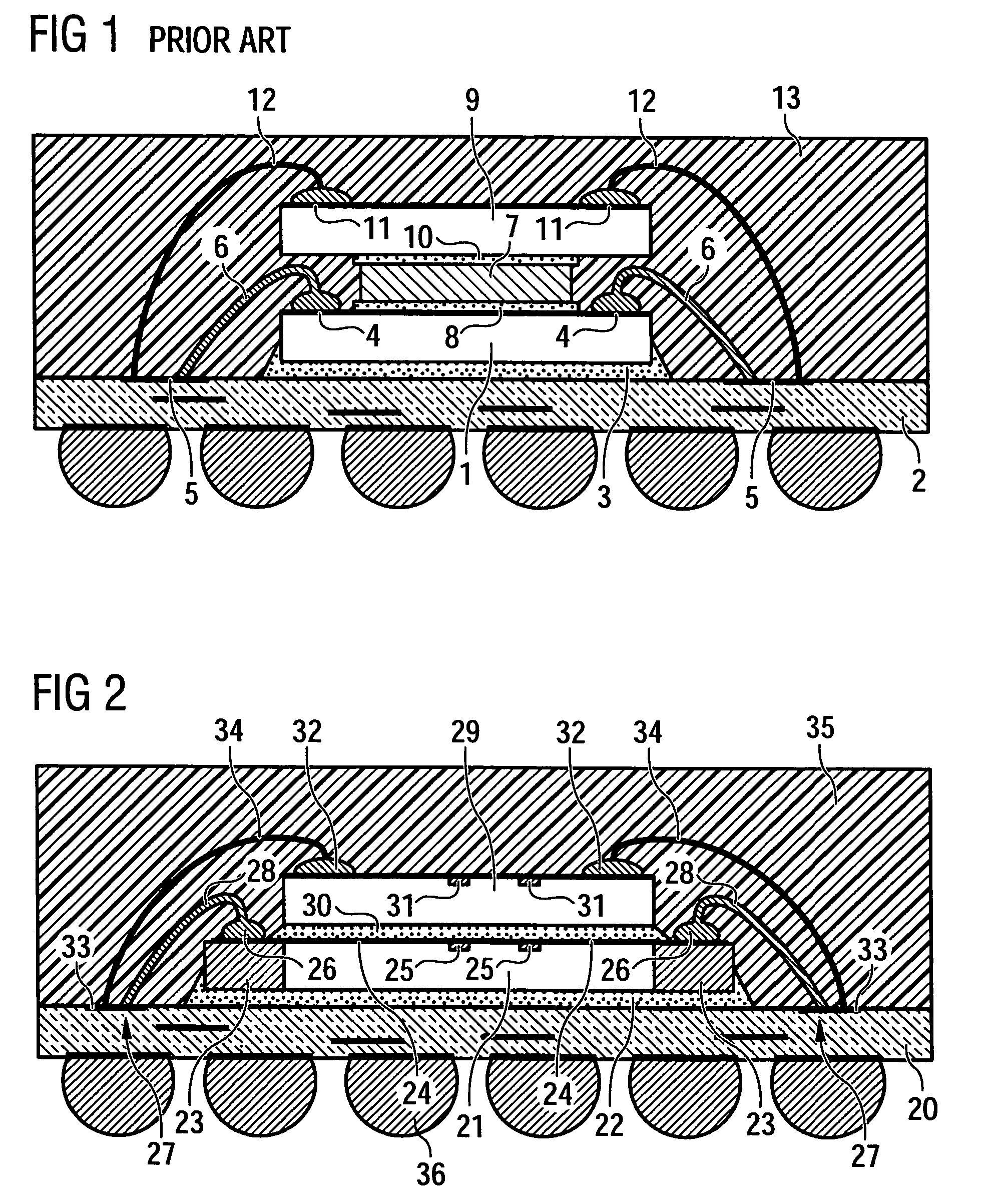
[0030]FIG. 2 illustrates an embodiment of the invention with an interposer board 20 with a reconstituted die 21 mounted on the interposer board 20. The reconstituted die 21 is mounted on the interposer board 20 by a liquid adhesive 22 or an adhesive tape 22. The reconstituted die 21 is provided with a frame 23 to increase the die area (fan-out) to the mentioned reconstituted die 21. The top or active surface of the reconstituted die 21 is provided with RDL layer 24, which reroute the bond pads 25 arranged in a center row on the reconstituted die 21 to wire bond pads 26 positioned on the frame 23. The wire bond pads 26 can be connected with landing pads 27 on the interposer board 20 by wire loops 28. This interconnection can also take place in a later step after assembly of the top die(s).

[0031]Then a second die 29 is die bonded on the top surface of the reconstituted die 21 with an adhesive glue or tape 30. This die 29 can also be a reconstituted die with a smaller fan-out area than...


PUM


Abstract

A stacked die package includes a substrate or interposer board that includes a contact area on a top surface and landing pads surrounding the contact area. Solder pads are disposed on an opposite side of the substrate. The solder pads are electrically connected with the landing pads by inner board wiring. A reconstituted die, which includes a die surrounded by a frame, is mounted over the substrate. A top die is mounted over the reconstituted die. Both the reconstituted die and the top die are electrically connected to the substrate, e.g., by wire bonds.

Description

TECHNICAL FIELD[0001]The invention relates to a stacked die package with integrated circuits such as memory devices or controllers.BACKGROUND[0002]The development of the application of integrated circuits shows that more complex functions are to be realized but there are limitations of the number of functions realizable on a single chip. Therefore, technologies for stacking of two or more dies with several functions and methods for the mechanical and electrical interconnection with one another or with a base substrate which is the basis for stacking and for mounting on a PCB (Printed Circuit Board) have been developed.[0003]Several technologies for contacting different chips are known. Conventional technologies are using chip and wire bonding for contacting the dies electrically. These are known processes with well-known parameters. Using these technologies for stacked dies (FBGA: fine ball grid array) the chips are placed one over another and the contacts of the dies are connected ...

Claims


Application Information

Patent Timeline
Patent Type & Authority Patents(United States)
IPC IPC(8): H01L21/782
CPCH01L21/568H01L21/6835H01L23/3128H01L24/33H01L24/49H01L24/83H01L24/85H01L24/96H01L24/97H01L25/50H01L2224/0401H01L2224/04105H01L2224/05644H01L2224/20H01L2224/32145H01L2224/32225H01L2224/48091H01L2224/48227H01L2224/48465H01L2224/4903H01L2224/49051H01L2224/73265H01L2224/83192H01L2224/8385H01L2224/85001H01L2224/97H01L2225/0651H01L2225/06527H01L2225/06555H01L2225/06593H01L2924/01004H01L2924/01005H01L2924/01014H01L2924/01028H01L2924/01029H01L2924/01078H01L2924/01079H01L2924/07802H01L2924/14H01L2924/15311H01L2924/19107H01L2924/00014H01L2224/82H01L24/48H01L2924/01006H01L2924/01033H01L2924/014H01L2224/78H01L2924/00H01L2924/00012H01L2924/10253H01L2924/15747H01L2924/181H01L24/73H01L2224/023H01L2224/45099H01L2224/05599H01L2924/0001
Inventor MEYER, TORSTENHEDLER, HARRY
Owner POLARIS INNOVATIONS LTD
Why Eureka
Try Eureka