Method for patterning thin film, method and apparatus for fabricating flat panel display

a thin film and flat panel display technology, applied in the field of flat panel display, can solve the problems of inconvenient installation, long process time, waste of photo-resist material and stripping solution, etc., and achieve the effect of reducing process time and minimizing pattern deformation

Active Publication Date: 2008-02-12
LG DISPLAY CO LTD
View PDF3 Cites 6 Cited by
  • Summary
  • Abstract
  • Description
  • Claims
  • Application Information

AI Technical Summary

Benefits of technology

[0019]An advantage of the present invention is to provide a fabrication method that is adaptive for conducting a patterning process without using a photolithography process, thereby reducing process time and minimizing pattern deformities.
[0020]In order to achieve these and other advantages of the invention, a method of fabricating a flat panel display comprises the steps of: forming a thin film on a substrate; applying an etch-resist solution having a solvent to the substrate; aligning a soft mold on the substrate; applying a first heat treatment to the etch-resist solution while applying a pressure to the soft mold on the etch-resist solution, the first heat treatment having a first temperature below a vaporization temperature of the solvent, thereby substantially forming a patterned etch-resist layer; separating the soft mold from the patterned etch-resist layer; applying a second heat treatment to the patterned etch-resist layer; and etching the thin film using the patterned etch-resist layer as a mask.
[0021]The method of fabrication further includes the step of forming an etch-resist solution before the step of applying an etch-resist solution.
[0022]In the method of fabrication, the etch-resist solution includes a solvent having about 40 wt %-60 wt %; a cross-linkable polymer resin having about 30 wt %-50 wt %; and a cross-linker having about 1 wt %-5 wt %.
[0023]In the method of fabrication, the cross-linkable polymer resin includes phenol-novolac resin.
[0024]In the method of fabrication, the cross-linker includes at least one of an amine family cross linker, a melamine family cross linker and a urea family cross linker.

Problems solved by technology

Traditional display devices include cathode ray tubes or Braun tubes, which make the display devices inconveniently large and heavy.
However, there is a problem in that the required time for the process is long, the photo-resist material and stripping solution is generally wasteful, and expensive equipment such as exposure equipment is required.

Method used


Image

  • Method for patterning thin film, method and apparatus for fabricating flat panel display
  • Method for patterning thin film, method and apparatus for fabricating flat panel display
  • Method for patterning thin film, method and apparatus for fabricating flat panel display

Examples


Embodiment Construction

[0053]Reference will now be made in detail to exemplary embodiments of the present invention, examples of which are illustrated in the accompanying drawings

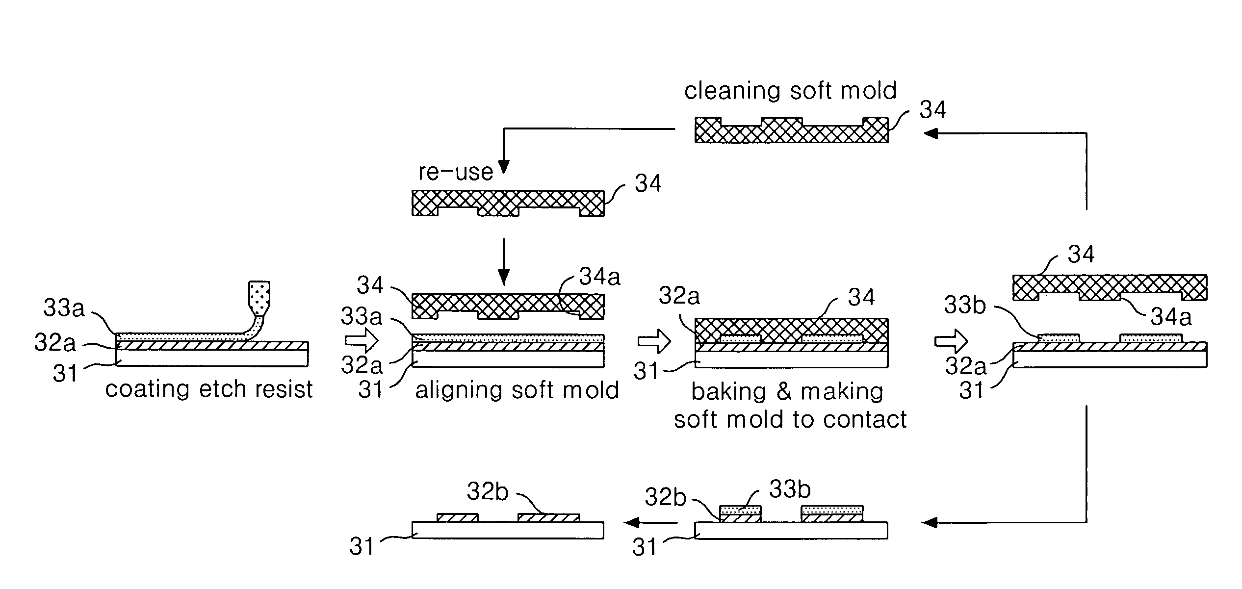
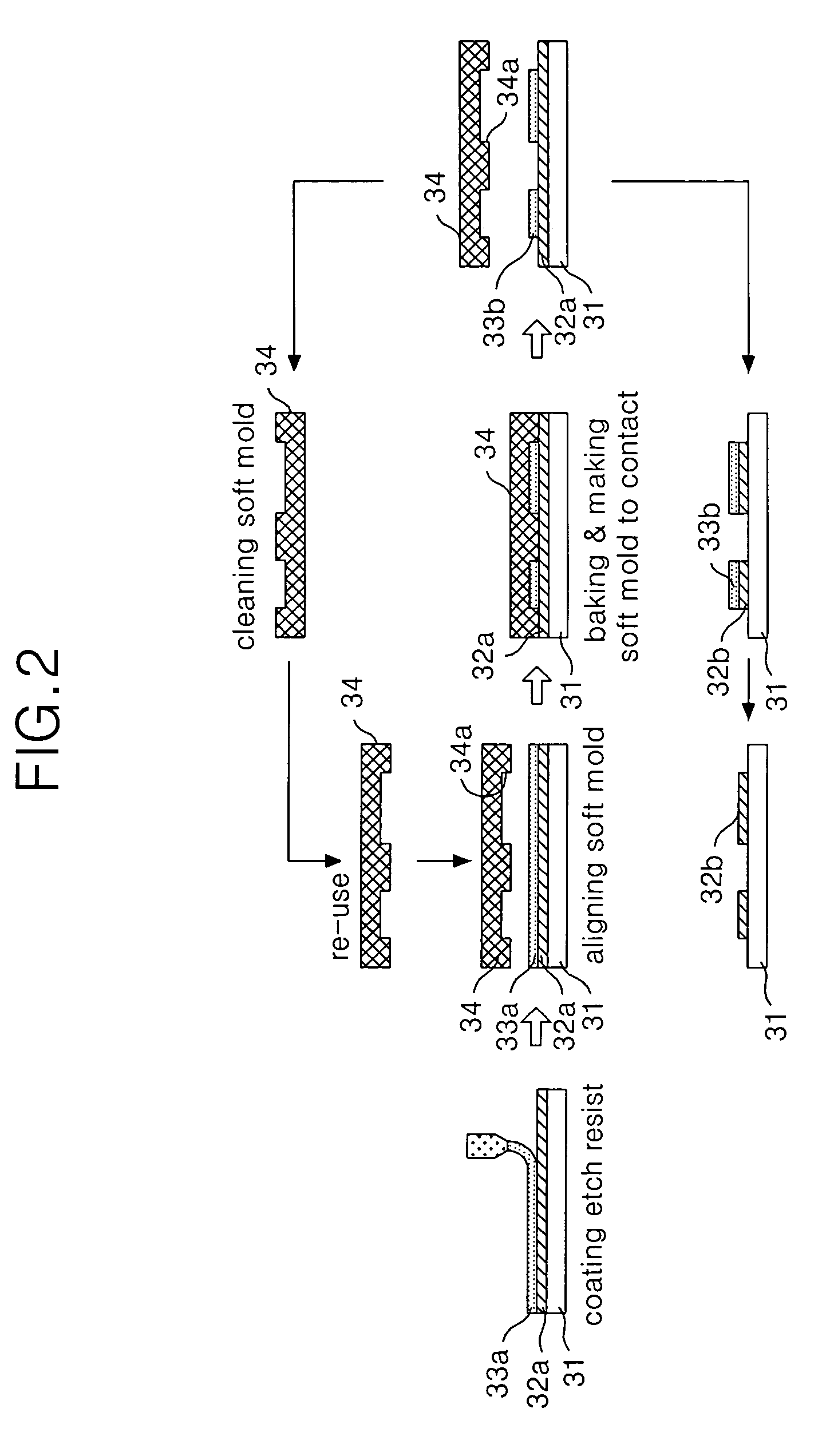
[0054]Hereinafter, the exemplary embodiments of the present invention will be described in detail with reference to FIGS. 2 to 6.

[0055]Referring to FIG. 2, an exemplary fabrication method of a flat panel display according to an embodiment of the present invention includes an etch-resist coating process in which an etch-resist solution 33a is substantially coated over a glass substrate 31 having a thin film 32a using a coating device; a process for patterning the etch-resist solution 33a using a soft mold 34; an etching process for the patterning the thin film 32a; a stripping process to remove the etch-resist pattern 33b and an inspection process for the patterned thin film layer 32b.

[0056]The thin film 32a of the pixel array formed on the glass substrate 31 may include a basic material such as that used for a patterned metal la...


PUM

PropertyMeasurementUnit
temperatureaaaaaaaaaa
pressureaaaaaaaaaa

Abstract

Disclosed is a method and apparatus for fabricating a patterned thin film layer within a flat panel display that employs a soft mold and heat treatment in place of a photolithographic process. The disclosed method may reduce process time as well as substantially minimize pattern deformities. A method of fabricating a thin film, a method and apparatus of fabricating a flat panel display according to an embodiment of the present invention includes the steps of forming a thin film on a substrate; coating an etch-resist solution including solvent over a substrate where the thin film has been formed; aligning a soft mold on the substrate provided with the etch-resist solution; forming a patterned etch-resist layer on the thin film by forming the etch-resist solution through a first heat treatment below the vaporization temperature of the solvent while pressure is applied to the soft mold on the etch-resist solvent; separating the soft mold from the patterned etch-resist layer; solidifying the patterned etch-resist layer through a second heat treatment; and etching the thin film by using the patterned etch-resist layer as a mask.

Description

[0001]This application claims the benefit of Korean Patent Application No. P2003-98129 filed on Dec. 27, 2003, which is hereby incorporated by reference for all purposes as if fully set forth herein.BACKGROUND OF THE INVENTION[0002]1. Field of the Invention[0003]The present invention relates to a flat panel display, and more particularly, to a method and apparatus for patterning a thin film, wherein the method and apparatus is adapted for patterning a thin film substantially without the use of photolithography, in a way that may reduce processing time and minimize pattern deformities.[0004]2. Description of the Related Art[0005]Display device are being emphasized more than ever as important visual information communication media. Traditional display devices include cathode ray tubes or Braun tubes, which make the display devices inconveniently large and heavy.[0006]Various display technologies have been developed toward replacing the cathode ray tube, and thereby making the display ...

Claims


Application Information

Patent Timeline
Patent Type & Authority Patents(United States)
IPC IPC(8): H01L21/31H01L21/027G02F1/13G02F1/136G03F7/00G09F9/00H01L21/00H01L51/00H01L51/56
CPCB82Y10/00B82Y40/00G03F7/0002H01L51/0014H01L51/56H10K71/20H10K71/00G02F1/13
Inventor KIM, YONG BUMKIM, JIN WUK
Owner LG DISPLAY CO LTD
Why Eureka
Try Eureka