Method and manufacturing surface acoustic wave device

Active Publication Date: 2008-02-19
TAIYO YUDEN KK +1
View PDF16 Cites 34 Cited by
  • Summary
  • Abstract
  • Description
  • Claims
  • Application Information

AI Technical Summary

Benefits of technology

[0014]It is therefore an object of the present invention to provide a method of manuf

Problems solved by technology

SAW devices, however, have a problem of passbands that shift with temperature.
However, these materials have a drawback of having poor stability with temperature.
On the other hand, crystal is a piezoelectric material that has excellent stability with temperature, but has a drawback of having a small electromechanical coupling coefficient.
With the substrate produced by forming a silicon oxide on the surface of a LT or LN substrate disclosed in Non-Patent Document 1, however, it is difficult to maintain the film quality and thickness of the silicon oxide film at a certain level, and frequency fluctuations can

Method used


Image

  • Method and manufacturing surface acoustic wave device
  • Method and manufacturing surface acoustic wave device
  • Method and manufacturing surface acoustic wave device

Examples


Example

First Embodiment

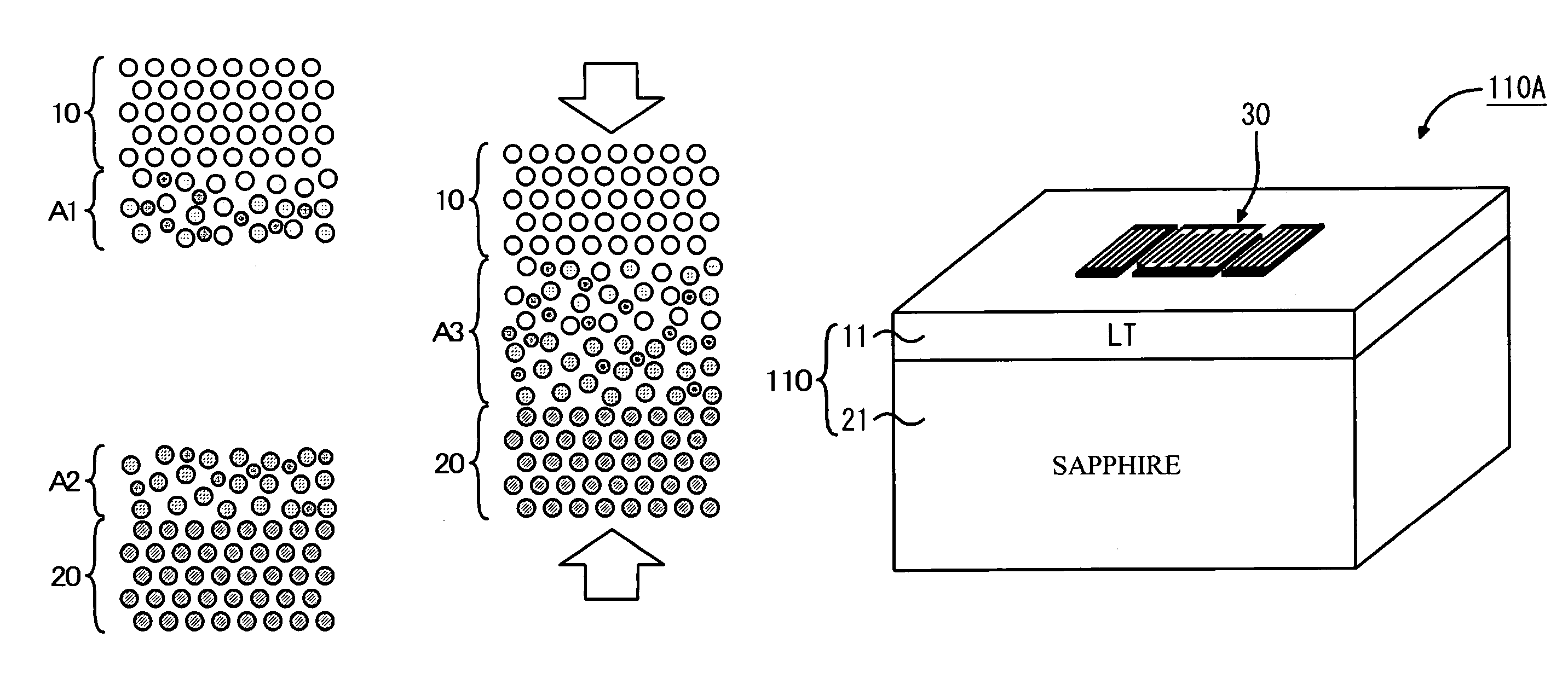
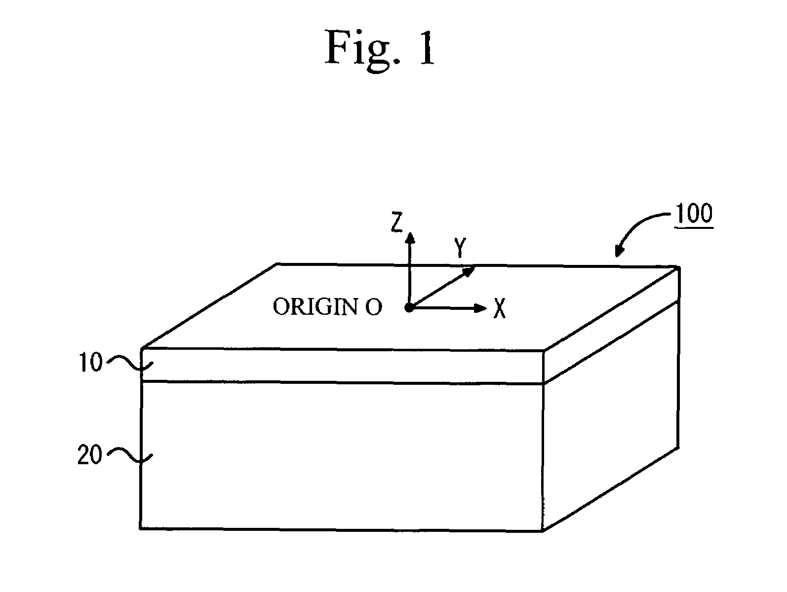
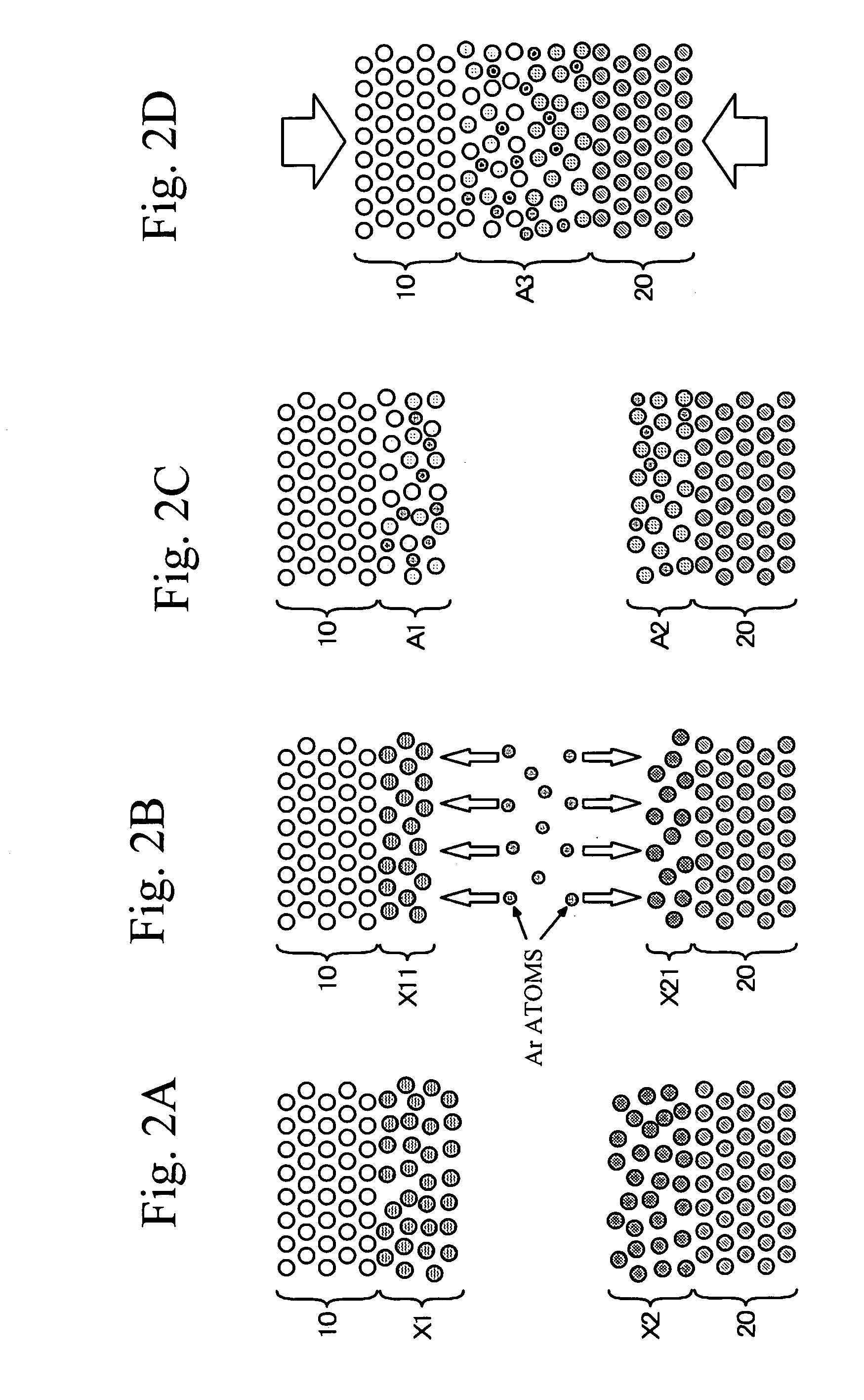
[0049]Referring to FIG. 1, a first embodiment of the present invention will be described. FIG. 1 is a schematic perspective view of a joined substrate 100 to be employed in a surface acoustic wave (SAW) device in accordance with this embodiment.

[0050]A piezoelectric substrate 10 is a piezoelectric single-crystal substrate of 42-degree Y-cut X-propagation lithium tantalate (hereinafter referred to as the “LT substrate”). The LT substrate has a SAW propagation direction X, and is a rotated Y-cut plate. In the LT substrate, the linear expansion coefficient in the SAW propagation direction X is 16.1 ppm / ° C. A supporting substrate 20 is a R-cut sapphire single-crystal substrate (hereinafter referred to as the “sapphire substrate”), for example. The linear expansion coefficient in the SAW propagation direction X is 5.3 ppm / ° C. The piezoelectric substrate 10 is 30 μm thick, and the supporting substrate 20 is 300 μm thick.

[0051]In this structure, the piezoelectric substra...

Example

Second Embodiment

[0066]In the first embodiment, the sapphire substrate 21 is employed as the supporting substrate 20. However, it is also possible to employ a SOS (silicon-on-sapphire) substrate 20A that has an intermediate film (a silicon thin film; see FIG. 6) containing silicon as a main component on the sapphire substrate 21. Referring to FIG. 6, this structure will be described below as a second embodiment of the present invention.

[0067]FIG. 6 is a perspective view of a SAW device 120A that includes the SOS substrate 20A in accordance with this embodiment.

[0068]As shown in FIG. 6, a joined substrate 120 of this embodiment has a silicon thin film 22 interposed between the sapphire substrate 21 and the LT substrate 11. In the SOS substrate 20A, the thickness of the sapphire substrate 21 is 300 μm, and the thickness of the silicon thin film 22 formed on the sapphire substrate 21 is approximately 1 μm.

[0069]The SOS substrate 20A can be formed through epitaxial growth of the silico...

Example

Third Embodiment

[0071]In the second embodiment, the SOS substrate 20A having the silicon thin film 22 interposed between the piezoelectric substrate 10 and the supporting substrate 20 increases the joining strength between the two substrates 10 and 20. However, it is also possible to increase the joining strength by forming an intermediate film containing a different material, as a main component, from the materials of the piezoelectric substrate 10 and the supporting substrate 20. The intermediate film should be formed on at least one of the joining surfaces of the piezoelectric substrate 10 and the supporting substrate 20, which are joined after the formation of the intermediate film. This structure will be described below as a third embodiment of the present invention, with reference to the accompanying drawings.

[0072]In a substrate joining process utilizing surface activation, there might be cases where adequate joining strength cannot be obtained by joining some materials dire...


PUM

PropertyMeasurementUnit
Purityaaaaaaaaaa

Abstract

A method of manufacturing a surface acoustic device that has a surface acoustic wave filter including comb-like electrodes, electrode pads, and wiring patterns formed on a joined substrate produced by joining a piezoelectric substrate and a supporting substrate to each other. This method includes the steps of: activating at least one of the joining surfaces of the piezoelectric substrate and the supporting substrate; and joining the piezoelectric substrate and the supporting substrate in such a manner that the activated joining surfaces face each other.

Description

BACKGROUND OF THE INVENTION[0001]1. Field of the Invention[0002]The present invention generally relates to a surface acoustic wave device and a method of manufacturing the surface acoustic wave device, and more particularly, to a method of manufacturing a surface acoustic wave device that includes a joined substrate.[0003]2. Description of the Related Art[0004]Surface acoustic wave (hereinafter referred to simply as SAW) devices are being widely used today as bandpass filters in communication devices such as portable telephones. In this trend, there has been an increasing demand for SAW filters with higher performances, as portable telephones has been becoming more and more sophisticated.[0005]SAW devices, however, have a problem of passbands that shift with temperature. To solve this problem and develop SAW devices having excellent stability with temperature has been a target to achieve in this field of technology in recent years.[0006]Materials for SAW devices are piezoelectric ma...

Claims


Application Information

Patent Timeline
IPC IPC(8): H04R17/10H01L41/09H01L41/18H01L41/22H01L41/312H01L41/39H03H3/08H03H9/02H03H9/25H03H9/64
CPCH03H3/08H03H9/02574Y10T29/49005Y10T29/49126Y10T29/42Y10T29/49016Y10T29/49007
Inventor MIURA, MICHIOMATSUDA, TAKASHISATOH, YOSHIOUEDA, MASANORITAKAGI, HIDEKI
Owner TAIYO YUDEN KK
Why Eureka
Try Eureka