Phase change memory cell and method of formation

a memory cell and phase change technology, applied in the field of semiconductor devices, can solve the problem that phase change memory cells require large operating currents, and achieve the effect of reducing power consumption

Active Publication Date: 2008-02-19
OVONYX MEMORY TECH LLC
View PDF223 Cites 59 Cited by
  • Summary
  • Abstract
  • Description
  • Claims
  • Application Information

AI Technical Summary

Benefits of technology

[0006]Embodiments of the invention provide a phase change memory element and methods for forming the same. The memory element includes a first electrode and a chalcogenide comprising phase change material layer over the first electrode. A metal-chalcogenide layer is over the phase change material layer. The metal chalcogenide layer comprises tin-telluride-telluride. A second electrode is over the metal-chalcogenide layer. The memory element is configured to have reduced power consumption.

Problems solved by technology

Often, however, phase change memory cells require large operating currents.

Method used


Image

  • Phase change memory cell and method of formation
  • Phase change memory cell and method of formation
  • Phase change memory cell and method of formation

Examples


Embodiment Construction

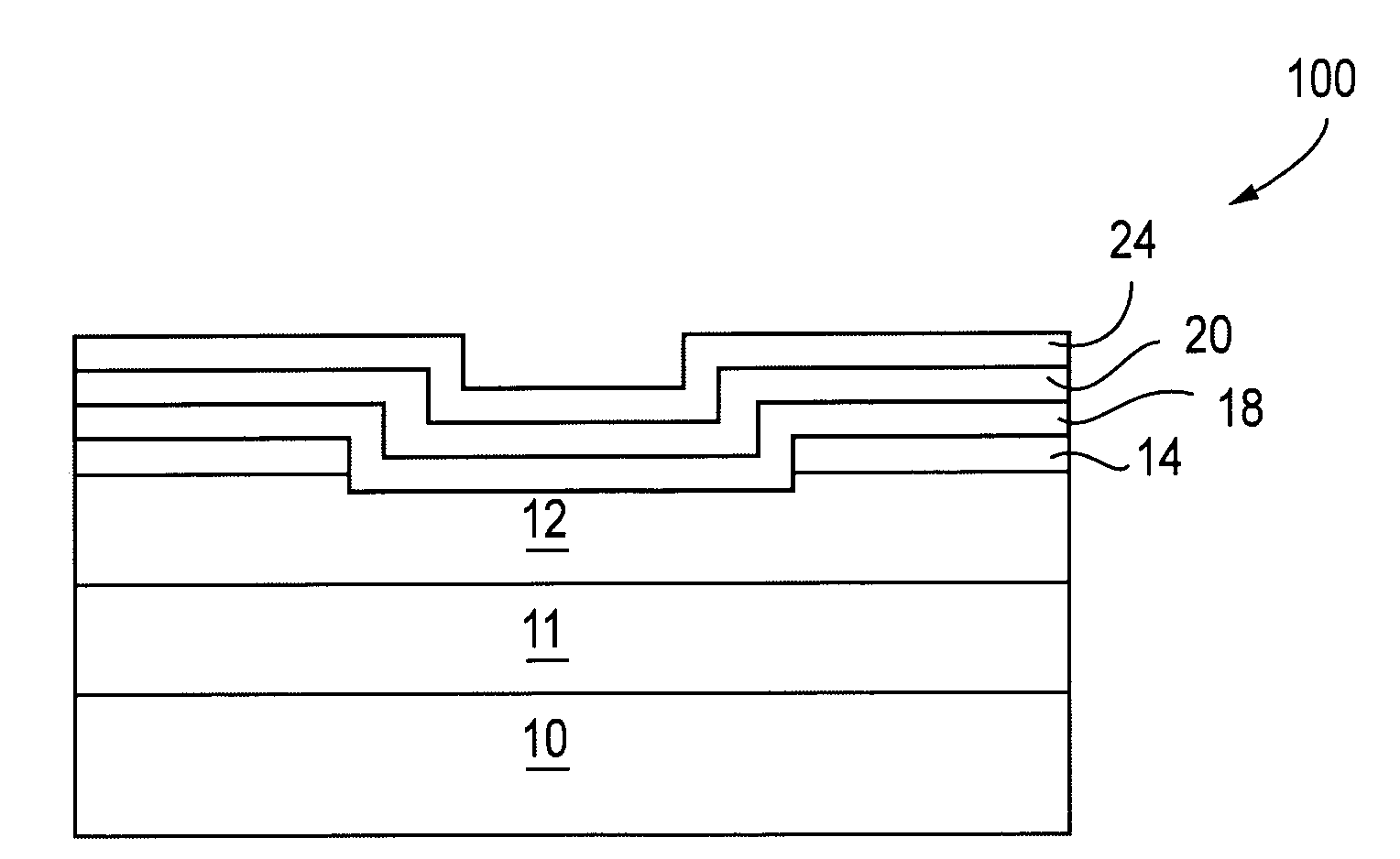
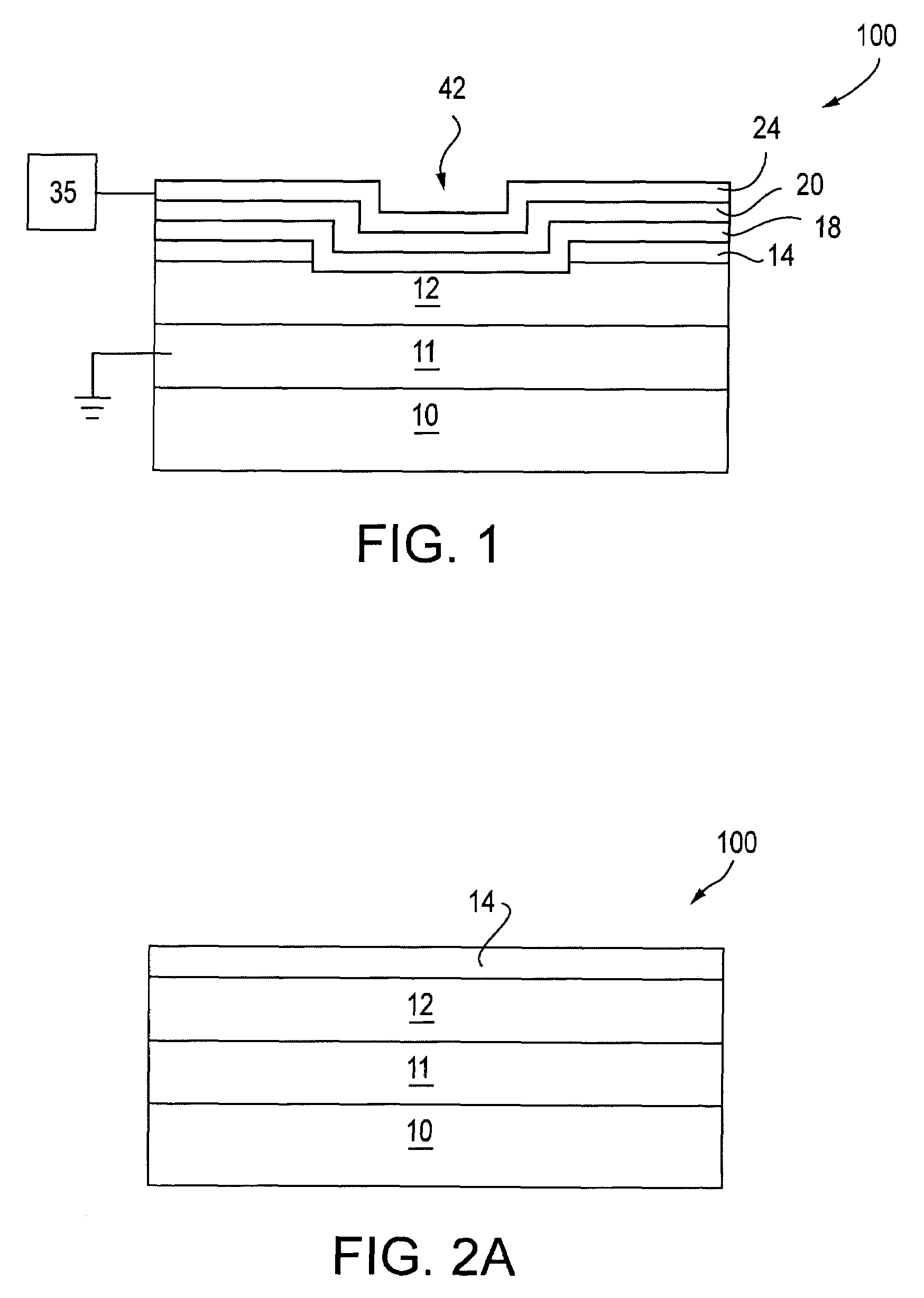
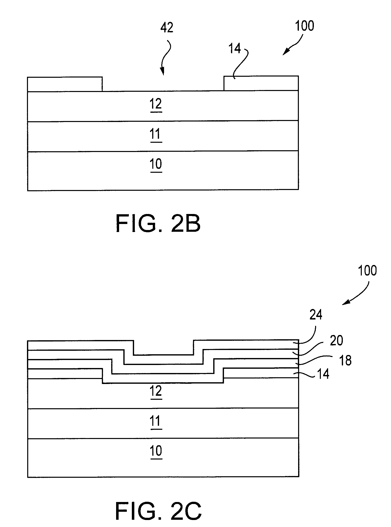
[0011]In the following detailed description, reference is made to various specific embodiments of the invention. These embodiments are described with sufficient detail to enable those skilled in the art to practice the invention. It is to be understood that other embodiments may be employed, and that various structural, logical and electrical changes may be made without departing from the spirit or scope of the invention.

[0012]The term “substrate” used in the following description may include any supporting structure including, but not limited to, a semiconductor substrate that has an exposed substrate surface. A semiconductor substrate should be understood to include silicon, silicon-on-insulator (SOI), silicon-on-sapphire (SOS), doped and undoped semiconductors, epitaxial layers of silicon supported by a base semiconductor foundation, and other semiconductor structures. When reference is made to a semiconductor substrate or wafer in the following description, previous process step...


PUM


Abstract

A phase change memory element and methods for forming the same are provided. The memory element includes a first electrode and a chalcogenide comprising phase change material layer over the first electrode. A metal-chalcogenide layer is over the phase change material layer. The metal chalcogenide layer is tin-telluride. A second electrode is over the metal-chalcogenide layer. The memory element is configured to have reduced current requirements.

Description

FIELD OF THE INVENTION[0001]The present invention relates to semiconductor devices, and in particular phase-change memory devices and method of forming the same.BACKGROUND OF THE INVENTION[0002]Non-volatile memories are important elements of integrated circuits due to their ability to maintain data absent a power supply. Phase change materials have been investigated for use in non-volatile memory cells. Phase change memory cells include phase change materials, such as chalcogenide alloys, which are capable of stably transitioning between amorphous and crystalline phases. Each phase exhibits a particular resistance state and the resistance states distinguish the logic values of the memory cell. Specifically, an amorphous state exhibits a relatively high resistance, and a crystalline state exhibits a relatively low resistance.[0003]A typical phase change cell has a layer of phase change material between first and second electrodes. As an example, the phase change material is a chalcog...

Claims


Application Information

Patent Timeline
Patent Type & Authority Patents(United States)
IPC IPC(8): H01L29/26
CPCH01L45/06H01L45/1233H01L45/144H10N70/231H10N70/826H10N70/8828H10N70/00
Inventor CAMPBELL, KRISTY A.
Owner OVONYX MEMORY TECH LLC
Why Eureka
Try Eureka