Non-volatile memory device with page buffer having dual registers and methods using the same

a memory device and register technology, applied in static storage, digital storage, instruments, etc., can solve the problem of wasting more time during the data transfer process, and achieve the effect of simplifying operation and significantly enhancing programing efficiency

Inactive Publication Date: 2008-02-26
CONVERSANT INTPROP MANAGEMENT INC
View PDF13 Cites 17 Cited by
  • Summary
  • Abstract
  • Description
  • Claims
  • Application Information

AI Technical Summary

Benefits of technology

[0011]The objective of the present invention is to provide a non-volatile memory device with a page buffer circuit having dual registers, by which data transfer between the two registers when programming can be omitted, so that the programming efficiency can be significantly enhanced. Moreover, for copy-back program function, only one register is active so that the operation can be simplified.
[0021]As mentioned above, the first and second registers of the page buffer circuit alternately perform programming. In addition, the first register performs programming and the second register stores data to be programmed at the same time for a cache program operation. As a result, the data transfer between two registers of the page buffer can be omitted, and the relevant control signals can be simplified. Moreover, a pre-charge process is not needed during a read operation for the memory cell array operated in a reverse direction, so memory access time and power consumption can be reduced.

Problems solved by technology

Moreover, it spends more time during the data transfer process.

Method used


Image

  • Non-volatile memory device with page buffer having dual registers and methods using the same
  • Non-volatile memory device with page buffer having dual registers and methods using the same
  • Non-volatile memory device with page buffer having dual registers and methods using the same

Examples


first embodiment

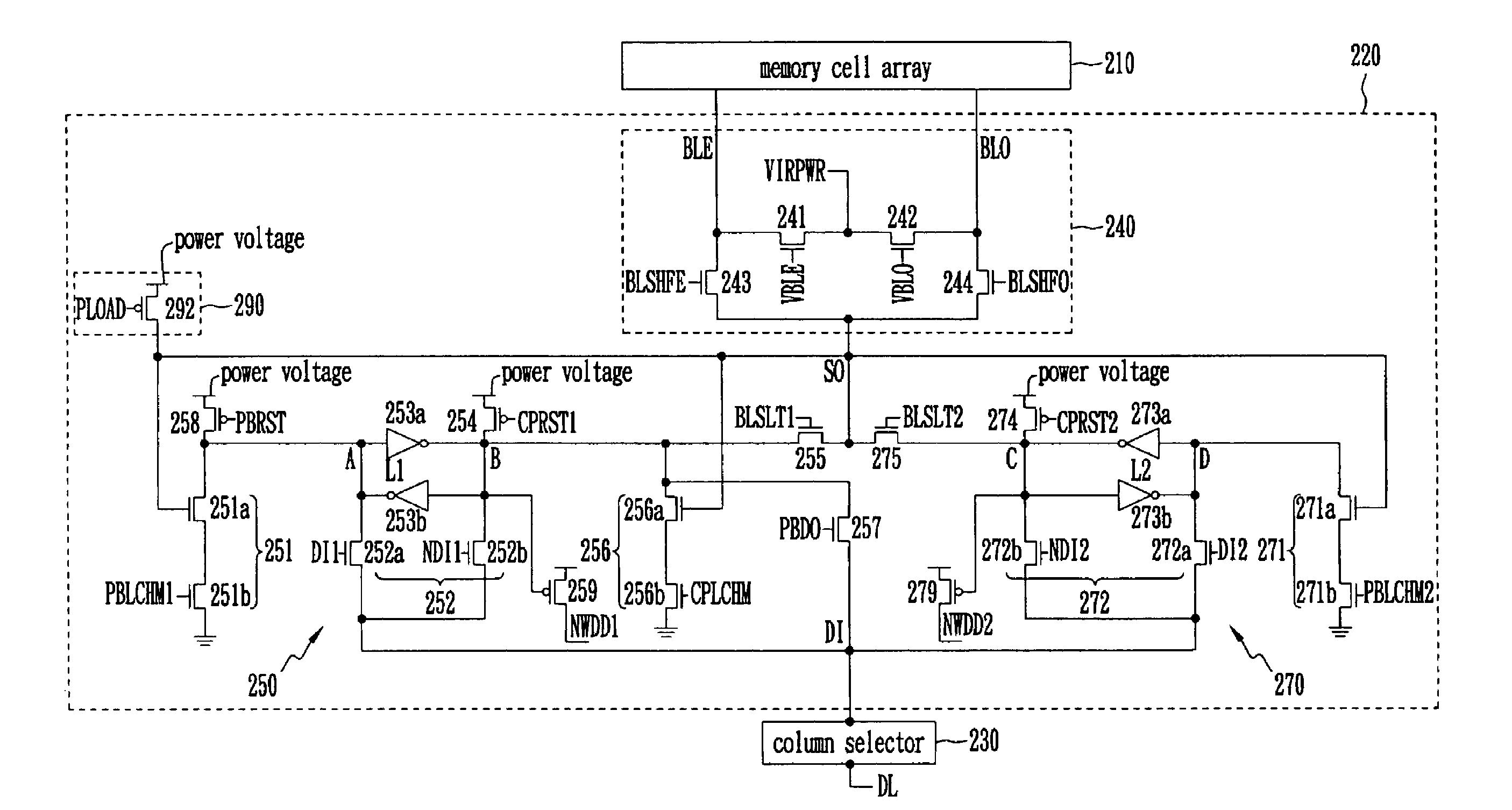
[0049]Referring to FIG. 3 and FIG. 4, a cache program method of the present invention is described. FIG. 3 shows command signals that are applied to the circuit of FIG. 2(c). The abscissa is divided into 9 segments, respectively labeled 1-9. FIG. 4 shows how data is transferred in the circuit of FIG. 2(c), which should be referred to along with FIG. 3 in the light of the labels.

[0050]At first (time segment 1), in order to pre-set latches L1 and L2 to a predetermined value, the PMOS transistors 254 and 274 are turned on by activating the control signals CPRST1 and CPRST2 logic low during a selected interval.

[0051]In time segment 2, the latch node B of the first register 250 is at a logic high state. The first set of data to be programmed is stored in the first latch L1. Data “1” or “0” in data line DL is thus stored to the latch L1 by activating the control signal DI1 or NDI1 logic high, respectively. In other words, the DI1 and NDI1 are in inverse states.

[0052]In time segment 3, the...

second embodiment

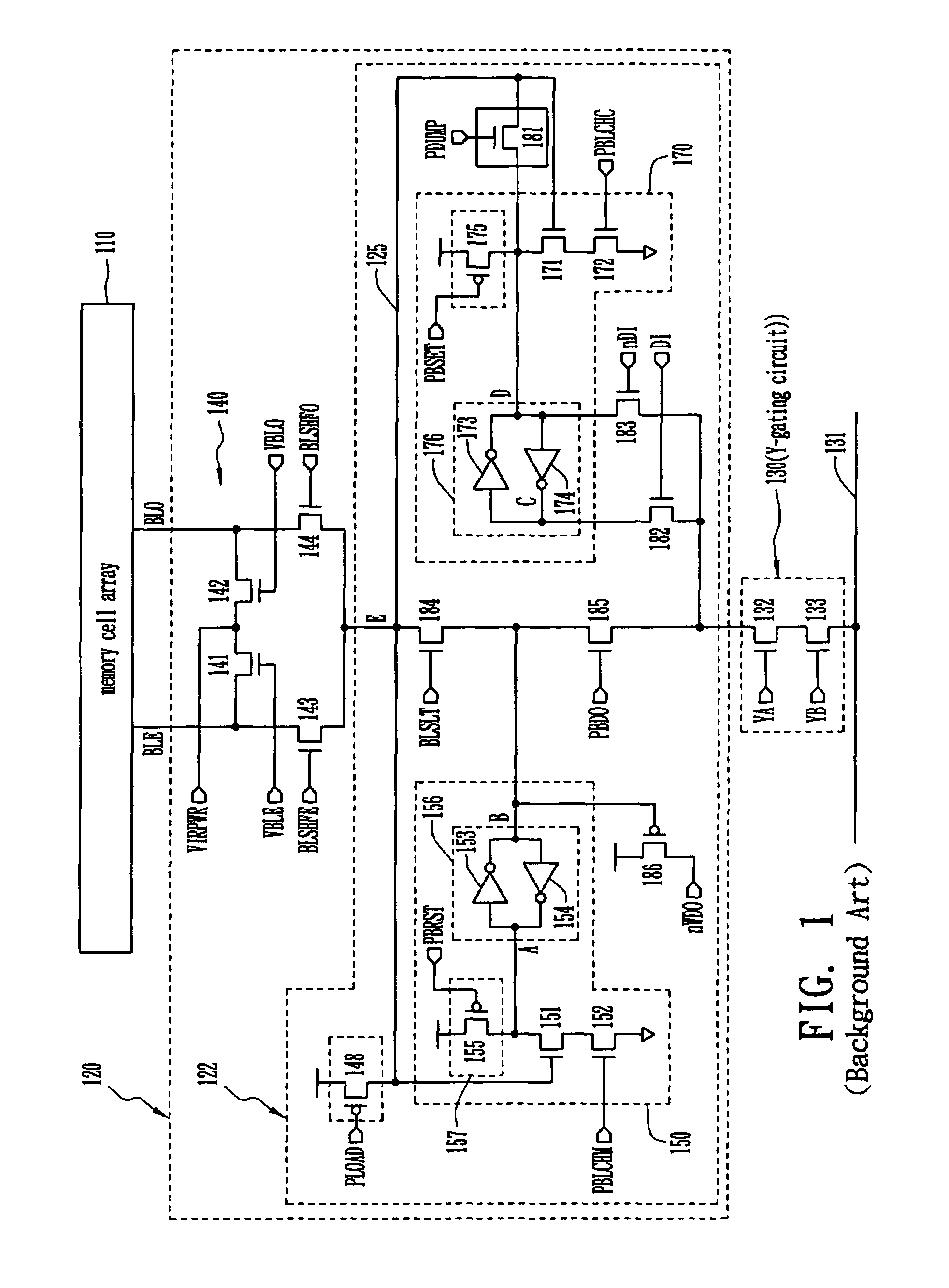
[0078]FIGS. 9(a), 9(b) and 10-15 illustrate the page buffer circuit and the methods thereof of the present invention, where a cell of NAND flash memory operates in a reverse direction. Referring to FIG. 9(a), a memory cell array 910 has a plurality of cell strings 9101. Each cell string 9101 comprises a first end P electrically connected to a corresponding page buffer circuit 920 through a bit line BLE or BLO, and a second end Q electrically connected to a common drain line (CDL). A cell string 9101 includes a string selection transistor ST1 coupled to a bit line BLE, a power voltage selection transistor ST2 coupled to a common drain line CDL, and memory cells M1-Mm serially coupled to the string selection transistor ST1 and the power voltage selection transistor ST2. The bit line BLE is connected to the source node of the memory cell M1 through the transistor ST1, the common drain line CDL is connected to the drain node of the memory cell Mm through the transistor ST2. The string s...


PUM


Abstract

A non-volatile memory device with a page buffer having dual registers includes a memory cell array, a selector circuit and a page buffer circuit, the selector circuit being coupled to an exterior data line, the page buffer circuit including a first register and a second register being coupled between the memory cell array and the selector circuit, and the first register and second register being commonly coupled through a sense node. The first and second registers alternately write data to the memory cell array for programming. As one of the first and second registers performs programming, the other register stores data from the data line concurrently. In other words, the second register stores data from the data line when the first register is in programming, whereas the first register stores data from the data line when the second register is in programming.

Description

RELATED U.S. APPLICATIONS[0001]Not applicable.STATEMENT REGARDING FEDERALLY SPONSORED RESEARCH OR DEVELOPMENT[0002]Not applicable.REFERENCE TO MICROFICHE APPENDIX[0003]Not applicable.FIELD OF THE INVENTION[0004]The present invention is related to a semiconductor memory device and, more specifically, to a non-volatile memory device with a page buffer circuit having dual registers and the methods using the same.BACKGROUND OF THE INVENTION[0005]U.S. Pat. No. 6,671,204, titled “non-volatile memory device with page buffer having dual registers and methods of using the same”, describes a page buffer design with cache program and copy-back functions. FIG. 1 illustrates the schematic diagram of Page Register and Sense Amplifier (S / A) block 120. The Page Register and S / A block 120 is coupled between a memory cell array 110 and a Y-gating circuit 130. The Page Register and Sense Amplifier (S / A) block 120 includes a bit line control circuit 140 and a page buffer 122. The page buffer 122 has a ...

Claims


Application Information

Patent Timeline
Patent Type & Authority Patents(United States)
IPC IPC(8): G11C7/10G11C16/04
CPCG11C7/1042G11C8/10G11C16/10G11C16/102G11C16/105G11C16/26G11C16/0483G11C2216/14
Inventor CHEN, CHUNG ZENWANG, JO YU
Owner CONVERSANT INTPROP MANAGEMENT INC
Why Eureka
Try Eureka