
Plasma processing device

Inactive Publication Date: 2008-03-04
TOKYO ELECTRON LTD
View PDF15 Cites 33 Cited by
  • Summary
  • Abstract
  • Description
  • Claims
  • Application Information

AI Technical Summary

Benefits of technology

[0012]It is, therefore, an object of the present invention to provide a plasma processing device capable of easily setting and controlling states of a multi-pole magnetic field according to the kinds of processing processes to be performed, thereby easily performing a proper process.
[0014]In accordance with another preferred embodiment of the present invention, there is provided a plasma processing device including: a processing chamber accommodating therein a substrate to be processed; a plasma generating mechanism installed in the processing chamber for performing a plasma process on the substrate to be processed; and a magnetic field forming mechanism for forming a multi-pole magnetic field around the substrate to be processed accommodated in the processing chamber, the magnetic field forming mechanism being constructed by arranging a plurality of magnet segments made of a permanent magnets and being installed outside the processing chamber, wherein at least parts of the magnet segments are rotated about respective vertical axes thereof to change magnetic pole directions thereof, thereby controlling strength of the multi-pole magnetic field formed around the substrate to be processed.
[0016]In accordance with still another preferred embodiment of the present invention, there is provided a plasma processing device including: a processing chamber accommodating therein a substrate to be processed; a plasma generating mechanism installed in the processing chamber for performing a plasma process on the substrate to be processed; and a magnetic field forming mechanism for forming a multi-pole magnetic field around the substrate to be processed accommodated in the processing chamber, the magnetic field forming mechanism being constructed by arranging a plurality of magnet segments made of a permanent magnets and being installed outside the processing chamber, wherein the magnetic field forming mechanism is separated into an upper magnetic field forming mechanism and a lower magnet field forming mechanism installed therebelow, and the upper and the lower magnetic field forming mechanism are moved vertically to move to and apart from each other, thereby controlling strength of the multi-pole magnetic field formed around the substrate to be processed in the processing chamber according to a type of to-be-etched layer formed on the substrate to be processed.
[0018]In accordance with still another preferred embodiment of the present invention, there is provided a plasma processing device including: a processing chamber accommodating therein a substrate to be processed; a plasma generating mechanism installed in the processing chamber for performing a plasma process on the substrate to be processed; and a magnetic field forming mechanism for forming a multi-pole magnetic field around the substrate to be processed accommodated in the processing chamber, the magnetic field forming mechanism being constructed by arranging a plurality of magnet segments made of a permanent magnets and being installed outside the processing chamber, wherein the magnet segments are allowed to be moved to and apart from the processing chamber, thereby controlling strength of the multi-pole magnetic field formed around the substrate to be processed in the processing chamber according to a type of to-be-etched layer formed on the substrate to be processed.

Problems solved by technology

In case of performing etching in this process without the multi-pole magnetic field, there is a non-uniformity of the etching rate, i.e., the etching rate is increased in a center region of the semiconductor wafer and decreased in a periphery portion thereof.
However, doing so increases power consumption and for such reason, permanent magnets are employed instead of the electromagnets in most devices.
However, in case of employing the permanent magnets, additional steps of attaching and detaching the magnetic field forming mechanism are required for formation and removal of the magnet field, which hinders facilitation of such processes.

Method used


Image

  • Plasma processing device
  • Plasma processing device
  • Plasma processing device

Examples


Embodiment Construction

[0036]Preferred embodiments of the present invention will be described in detail with reference to the accompanying drawings.

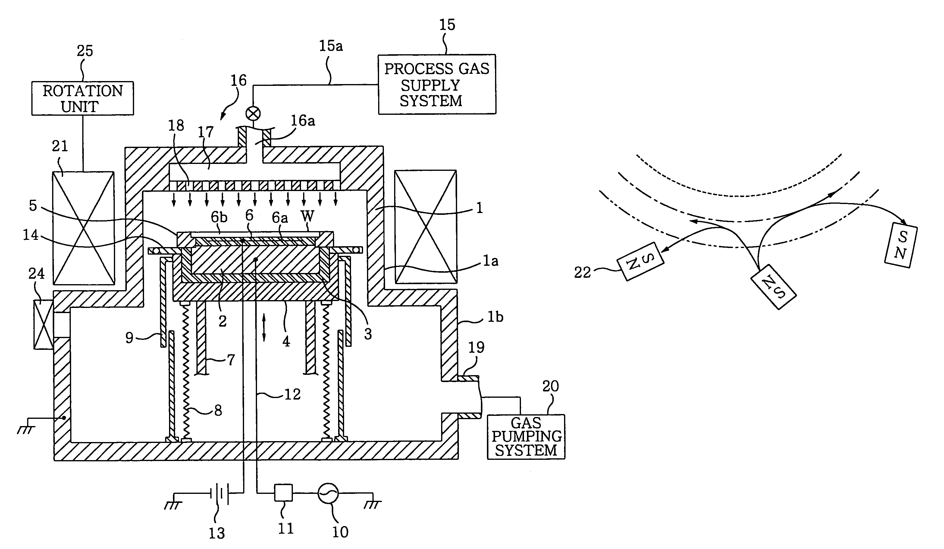
[0037]FIG. 1 is a schematic diagram illustrating a configuration of a plasma processing device for etching a semiconductor wafer in accordance with a preferred embodiment of the present invention. A reference numeral 1 in FIG. 1 represents a vacuum chamber made of, e.g., aluminum, and configured to air-tightly seal an inner space thereof. The vacuum chamber 1 has a cylindrical shape and the inner space thereof is used as a plasma processing chamber.

[0038]The vacuum chamber 1 has a stepped cylindrical shape with an upper portion 1a having a smaller diameter and a lower portion 1b having a larger diameter and is connected to a ground potential. Further, installed in the vacuum chamber 1 is a supporting table (a susceptor) 2 for substantially horizontally supporting a semiconductor wafer W serving as a substrate to be processed having a to-be-processed surface th...


PUM

PropertyMeasurementUnit
Angleaaaaaaaaaa
Electric chargeaaaaaaaaaa
Currentaaaaaaaaaa

Abstract

Each magnet segment 22 of a magnetic field forming mechanism 21 is constructed such that, after the magnetic pole of each magnet segment 22 set to face a vacuum chamber 1 as shown in FIG. 3A, adjoining magnet segments 22 are synchronously rotated in opposite directions, and hence every other magnet element 22 is rotated in the same direction as shown in FIGS. 3B, 3C to thereby control the status of a multi-pole magnetic field formed in the vacuum chamber 1 and surrounding a semiconductor wafer W. Therefore, the status of a multi-pole magnetic field can be easily controlled and set appropriately according to a type of plasma processing process to provide a good processing easily.

Description

FIELD OF THE INVENTION[0001]The present invention relates to a plasma processing device; and, more particularly, to a plasma processing device for performing a plasma processing such as etching on a substrate to be processed, e.g., a semiconductor wafer.BACKGROUND OF THE INVENTION[0002]In a field of manufacturing semiconductor devices, a plasma processing device has been used to perform a predetermined processing (e.g., etching or film formation) on a substrate to be processed (e.g., a semiconductor wafer) accommodated in a processing chamber by applying a plasma generated in the processing chamber thereto.[0003]In such a plasma processing device, a state of the plasma needs to be kept suitable for the plasma processing in order to perform a good processing. For such reason, conventionally there are numerous plasma processing devices incorporating therein a magnetic field forming mechanism which forms a magnetic field for controlling the plasma.[0004]There are known a dipole type an...

Claims


Application Information

Patent Timeline
IPC IPC(8): H01L21/00H05H1/46C23F1/00H01J37/32H01L21/205H01L21/302H01L21/3065H01L21/31
CPCH01J37/32623H01J37/32688H01L21/302
Inventor ONO, HIROOTATESHITA, KOICHIHONDA, MASANOBUNAGASEKI, KAZUYAHAYASHI, DAISUKE
Owner TOKYO ELECTRON LTD
Features
  • Generate Ideas
  • Intellectual Property
  • Life Sciences
  • Materials
  • Tech Scout
  • Unparalleled Data Quality
  • Higher Quality Content
  • 60% Fewer Hallucinations
Learn More