Technique for combining scan test and memory built-in self test

a technology of scan test and self-testing, which is applied in the direction of digital storage, measurement devices, instruments, etc., can solve the problems of low efficiency, low efficiency, and often under-estimation of the cost and effort required to obtain reliable data with respect to proper functionality and reliability of the device, so as to improve switching activity, reduce the time required for testing a specified circuitry, and improve the effect of efficiency

Active Publication Date: 2008-03-04
GLOBALFOUNDRIES US INC
View PDF14 Cites 32 Cited by
  • Summary
  • Abstract
  • Description
  • Claims
  • Application Information

AI Technical Summary

Benefits of technology

[0018]Generally, the present invention is directed to a technique that enables simultaneous performance of a scan test of a logic circuitry portion and a memory test of an embedded memory, wherein, compared to a conventional semiconductor device, additional input lines and output lines for the test specific hardware resources on the chip may be avoided. To this end, the present invention is based on the concept that at least one scan flip-flop is selected for controlling, for instance for starting and stopping, an MBIST logic when the circuit is in the scan test mode. Hence, the time required for testing a specified circuitry may significantly be reduced, while advantageously the increased switching activity during the scan test mode provides high efficiency during stress tests, since test data is written into each memory cell and is read back again, while the high switching activity in the combinatorial logic portion of the circuitry still continues.

Problems solved by technology

In manufacturing semiconductor devices including a relatively complex circuitry, the testing of the device may represent a part of the manufacturing process, which is frequently under-estimated in terms of cost and effort required to obtain reliable data with respect to proper functionality and reliability of the device.
One reason in failing to meet performance specifications of the integrated circuit may reside in design errors that may be identified and remedied by circuit verification on the basis of software simulation and / or prototype testing prior to mass production of the integrated circuits under consideration.
An improper functionality of the integrated circuit may further be caused by the manufacturing process itself when the completed circuitry does not correspond to the verified circuit design owing to process fluctuations in one or more of a large number of process steps.
Although measurement and test procedures are incorporated at many points in the manufacturing process, it is nevertheless extremely important to ascertain the correct functioning of the final semiconductor device, since, according to a common rule of thumb, the costs caused by defective chips increase with each assembly phase by approximately one order of magnitude.
For example, the costs caused by a defective circuit board including a faulty chip are typically significantly higher than identifying a defective chip prior to shipping and assembling the circuit board.
The same holds true for a system, when a failure thereof is caused by one or more defective circuit boards as a downtime of an industrial system may result in averaged costs of approximately several hundred dollars per minute compared to a price of a few dollars for an integrated circuit chip having caused the defect.
As discussed above, economic constraints force semiconductor manufacturers to not only minimize the defect level of the total manufacturing process, but also to provide, in combination with a reduced defect level, a high fault coverage to reduce the delivery of defective chips at reasonable cost for appropriate test procedures and techniques.
However, the fault coverage, i.e., the potential for identifying any error within the functional logic, significantly depends on the design, selection and number of appropriate scan chains and suitable input vectors.
Due to the configuration of the device 100, the scan test and the memory test have to be sequentially performed, thereby requiring a moderately high amount of test time.
However, merely providing additional scan flip-flops for the MBIST logic 130 and incorporating these additional scan flip-flops into the scan chain 140 may significantly complicate the situation during testing of the device 100, as the scan test and the memory test mutually depend on each other.
Moreover, the conventional technique as described with reference to FIGS. 1a and 1b may not be very efficient during stress tests in which a high switching activity is required in the combinatorial logic, i.e., the logic circuitry portion 110, while test data are written into and read out from the memory to verify a correct function of the memory during specified stress conditions.

Method used


Image

  • Technique for combining scan test and memory built-in self test
  • Technique for combining scan test and memory built-in self test
  • Technique for combining scan test and memory built-in self test

Examples


Embodiment Construction

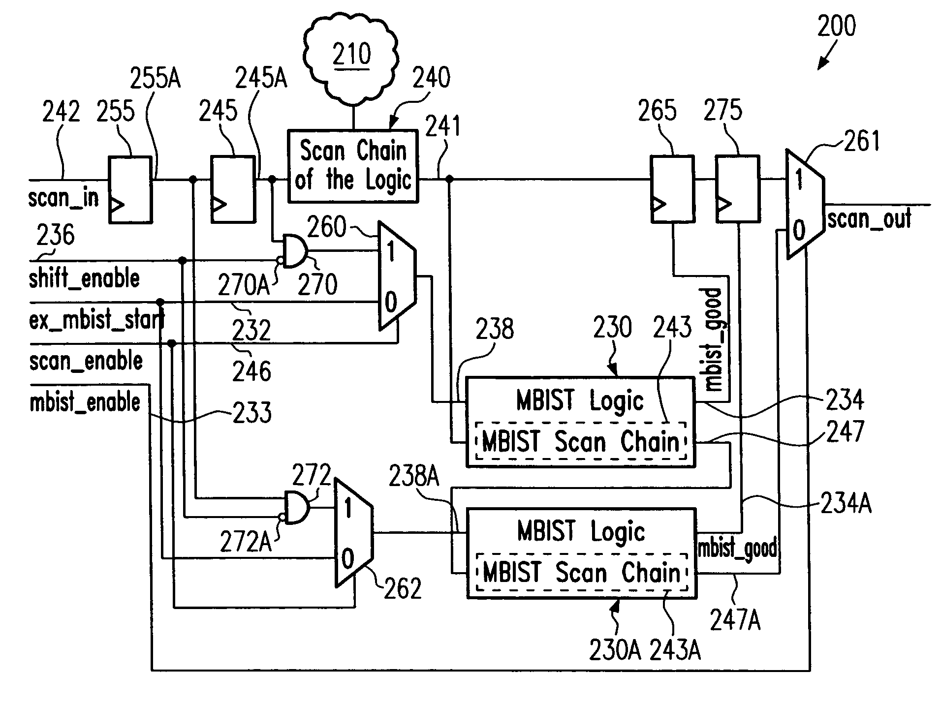
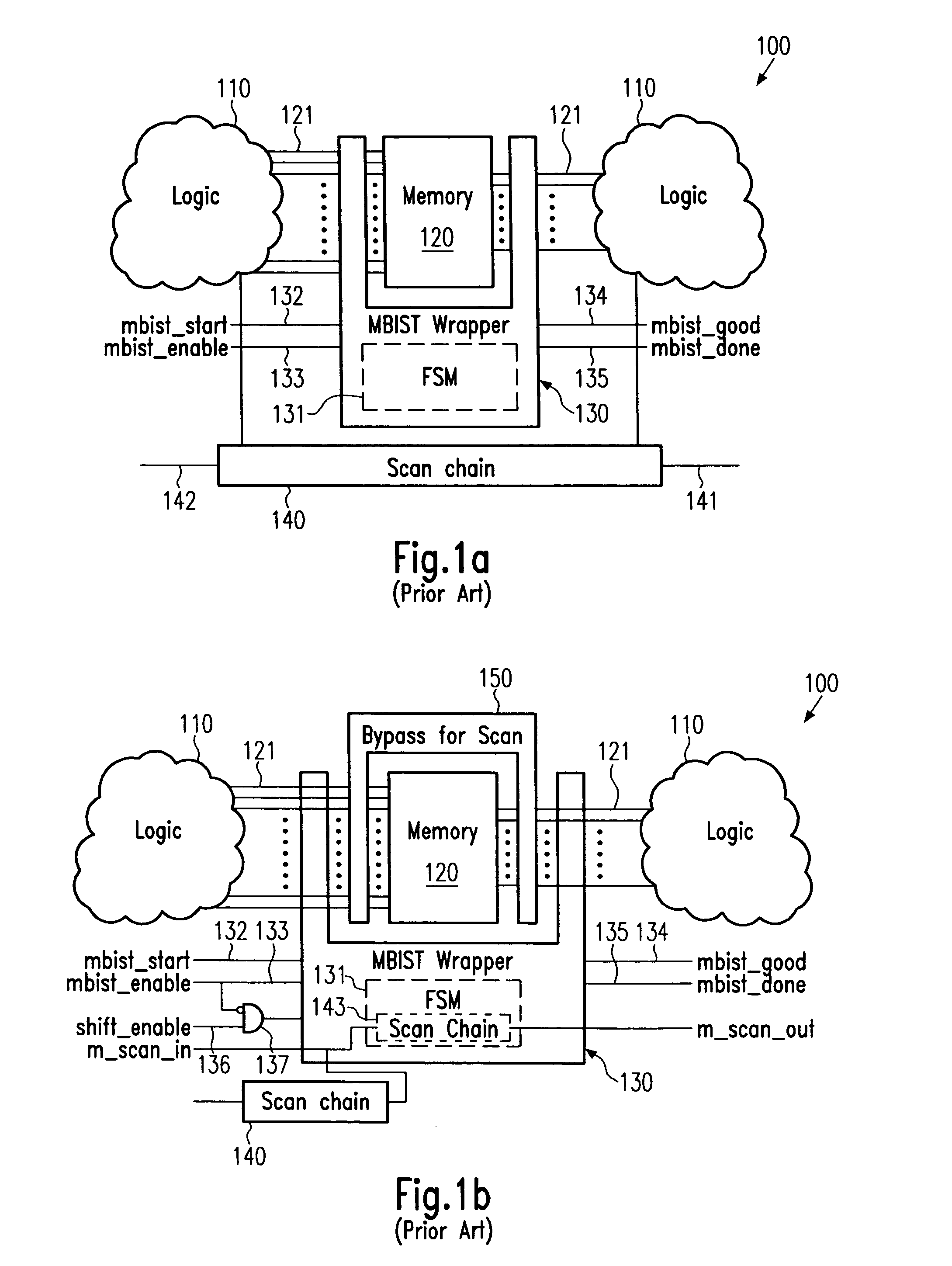
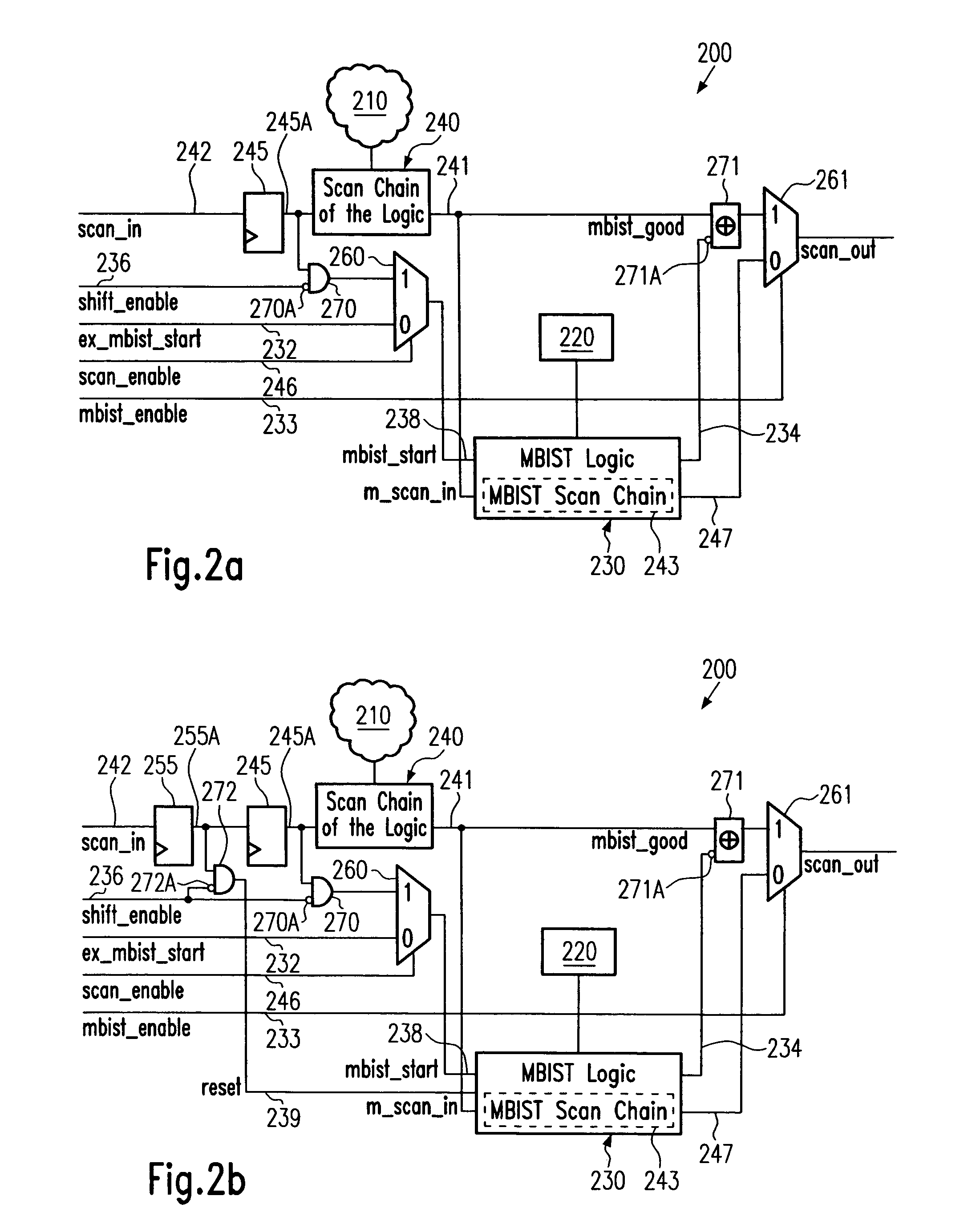
[0027]Illustrative embodiments of the invention are described below. In the interest of clarity, not all features of an actual implementation are described in this specification. It will of course be appreciated that in the development of any such actual embodiment, numerous implementation-specific decisions must be made to achieve the developers' specific goals, such as compliance with system-related and business-related constraints, which will vary from one implementation to another. Moreover, it will be appreciated that such a development effort might be complex and time-consuming, but would nevertheless be a routine undertaking for those of ordinary skill in the art having the benefit of this disclosure.

[0028]The present invention will now be described with reference to the attached figures. Various structures, systems and devices are schematically depicted in the drawings for purposes of explanation only and so as to not obscure the present invention with details that are well ...


PUM


Abstract

Semiconductor devices including logic circuitry and embedded memories may be tested using one or more flip-flops in a scan chain that are connected to a control input of an MBIST logic, thereby allowing the control of the MBIST logic during a simultaneous scan test and memory test run. By combining the output of the MBIST logic with the output of the scan chain, fault diagnosis is maintained.

Description

BACKGROUND OF THE INVENTION[0001]1. Field of the Invention[0002]The present invention generally relates to techniques for testing semiconductor devices, and, more particularly, to techniques for testing integrated circuits that include logic circuitry portions and embedded memory portions with respective scan chains and memory built-in self test logics connected thereto.[0003]2. Description of the Related Art[0004]In manufacturing semiconductor devices including a relatively complex circuitry, the testing of the device may represent a part of the manufacturing process, which is frequently under-estimated in terms of cost and effort required to obtain reliable data with respect to proper functionality and reliability of the device. One reason in failing to meet performance specifications of the integrated circuit may reside in design errors that may be identified and remedied by circuit verification on the basis of software simulation and / or prototype testing prior to mass production...

Claims


Application Information

Patent Timeline
Patent Type & Authority Patents(United States)
IPC IPC(8): G01R31/28G11C29/00G11C7/00G01R31/3187
CPCG01R31/318544G11C29/32G01R31/318555
Inventor SEURING, MARKUS
Owner GLOBALFOUNDRIES US INC
Why Eureka
Try Eureka