Integrated circuit binning and layout design system

a layout design and integrated circuit technology, applied in the direction of cad circuit design, program control, instruments, etc., can solve the problems of not allowing the prediction of cross-coupling (i.e., noise) between wire paths and propagation delays (i.e. timing), known routing tools are often blind to the power distribution requirements of the design, and tools often do not allow alternate assignmen

Active Publication Date: 2008-03-04
ORACLE INT CORP
View PDF11 Cites 10 Cited by
  • Summary
  • Abstract
  • Description
  • Claims
  • Application Information

AI Technical Summary

Benefits of technology

[0010]In accordance with the present invention, a binning methodology and layout design methodology is provided. The binning methodology includes a table setting forth specific widths of signal wires and the corresponding spacing to shield wires. The shield wires are adjacent and on both sides of a routed signal wire. The effect on timing, noise, and power distribution

Problems solved by technology

However, arbitrary routing, as generated by known routing tools, often does not allow the prediction of cross-coupling (i.e., noise) between wire paths and propagation delays (i.e., timing) within a wire path.
Known routing tools are often blind to power distribution requirements of the design.
Known routing tools might create dense routing regions

Method used


Image

  • Integrated circuit binning and layout design system
  • Integrated circuit binning and layout design system
  • Integrated circuit binning and layout design system

Examples


Embodiment Construction

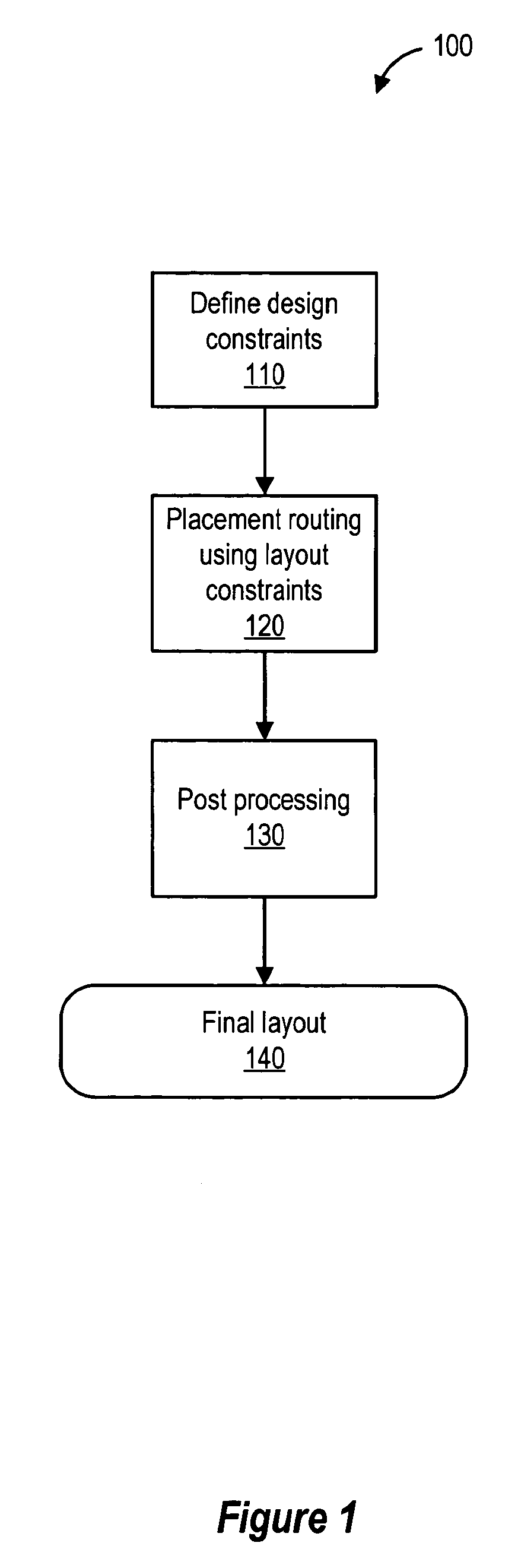
[0025]Referring to FIG. 1, the operation of a system 100 for generating a correct by construction layout is shown. The system 100 starts by defining design constraints to be used within the binning and layout methodology at step 110. Next, the system places routing of an integrated circuit design using the binning and layout design constraints at step 120. After the binning and layout design is completed, the system performs a post processing operation on the binning and layout design at step 130. After the post processing operation is completed, a final design is provided by the system 100 at step 140.

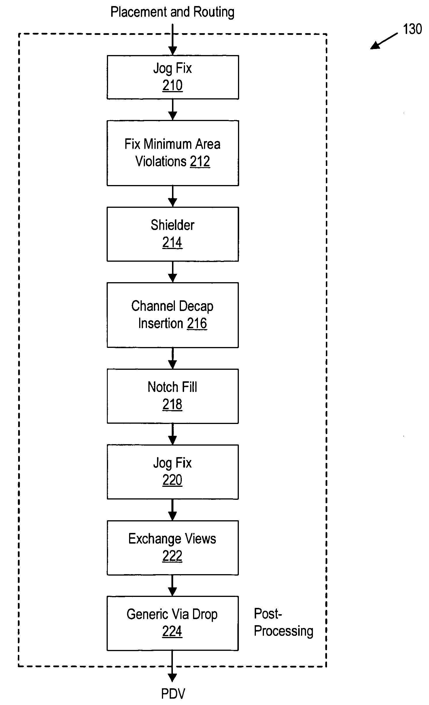
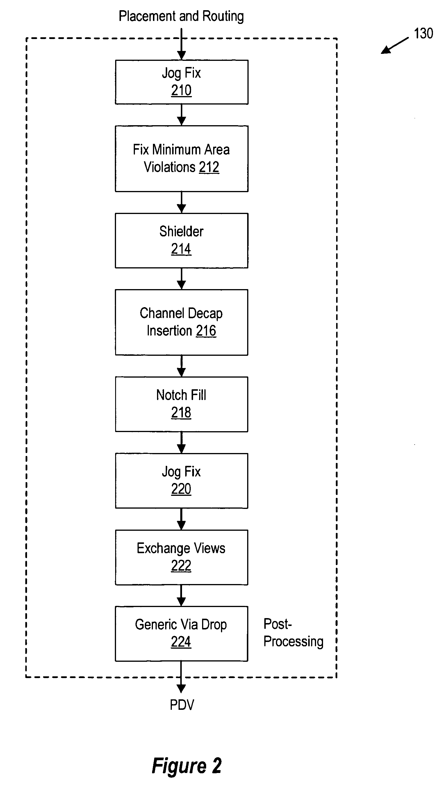
[0026]Referring to FIG. 2, a flow chart of the operation of a layout post processing module 130 is shown. More specifically, once a top level layout is substantially completely routed (and repeater inserted where applicable), the layout post processing (LPP) flow is executed to assure that a design complies with various design rules, EM / IR constraints, and noise constraints. The LPP f...


PUM


Abstract

A method for binning and layout of an integrated circuit design which includes providing a table setting forth predefined widths of signal wires and corresponding spacing to shield wires, characterizing effects on timing, noise, and power distribution based on predefined widths and spacing combinations as functions of the length of the signal wire, and laying out the integrated circuit design based upon the predefined widths of signal wires and corresponding spacing to shield wires. The shield wires are adjacent and on both sides of the routed signal wire.

Description

BACKGROUND OF THE INVENTION[0001]1. Field of the Invention[0002]The present invention relates to signal path layout and routing and more particularly to binning layout.[0003]2. Description of the Related Art[0004]An integrated circuit typically includes a plurality of generally horizontal layers, each layer having a plurality of components. The components that are to be connected on an integrated circuit form a net, while any component not connected to a particular net is considered to be an obstruction to that net.[0005]One step in the design of an integrated circuit is to select the wire paths to connect the components. The path of the actual connection between the components, known as the wire path, is then defined as the route via which the components are connected.[0006]It is known to use routing tools to provide the path for the actual connection between the components. However, arbitrary routing, as generated by known routing tools, often does not allow the prediction of cros...

Claims


Application Information

Patent Timeline
IPC IPC(8): G06F17/50G06F9/45
CPCG06F17/5068G06F30/39
Inventor HOEROLD, STEPHANDUTT, ARJUN
Owner ORACLE INT CORP
Why Eureka
Try Eureka