Method for producing semi-conducting devices and devices obtained with this method

Inactive Publication Date: 2008-03-18
OERLIKON SOLAR AG (TRUEBBACH)
View PDF24 Cites 3 Cited by
  • Summary
  • Abstract
  • Description
  • Claims
  • Application Information

AI Technical Summary

Benefits of technology

[0014]The object of the present invention is to provide a method for producing semiconductors with a particular application in solar cells, avoiding cross-contamination by doping agents and exempt of disadvantages above mentioned.

Problems solved by technology

However, in a single chamber deposition process of a p-i-n solar cell, for example, the subsequent deposition of the i-layer on the p-layer may cause boron recycling from the reactor walls and from the deposited p-layer.
As a result, boron will contaminate the i-layer at the critical p-i interface and thereby weaken the strength of the electrical field in the i-layer close to p-i interface.
This provokes a less efficient carrier separation just in this zone and leads to a reduced collection efficiency in the solar cell and thereby to a deterioration of the cell performance.
However, the higher investment in multi-chamber systems equipment becomes a drawback particularly in the field of solar cells where costs are a major issue.
Similar problems exist with n-i-p solar cells in which phosphor used to dope the n-layer contaminates the i-layer at the critical n-i interface.
Different treatments have been tested with encouraging results, but they still leave open the question of the light-induced degradation of these solar cells, they use expensive gases, they have long treatment durations or are incompatible with large area deposition in industrial reactors.

Method used


Image

  • Method for producing semi-conducting devices and devices obtained with this method
  • Method for producing semi-conducting devices and devices obtained with this method

Examples


first embodiment

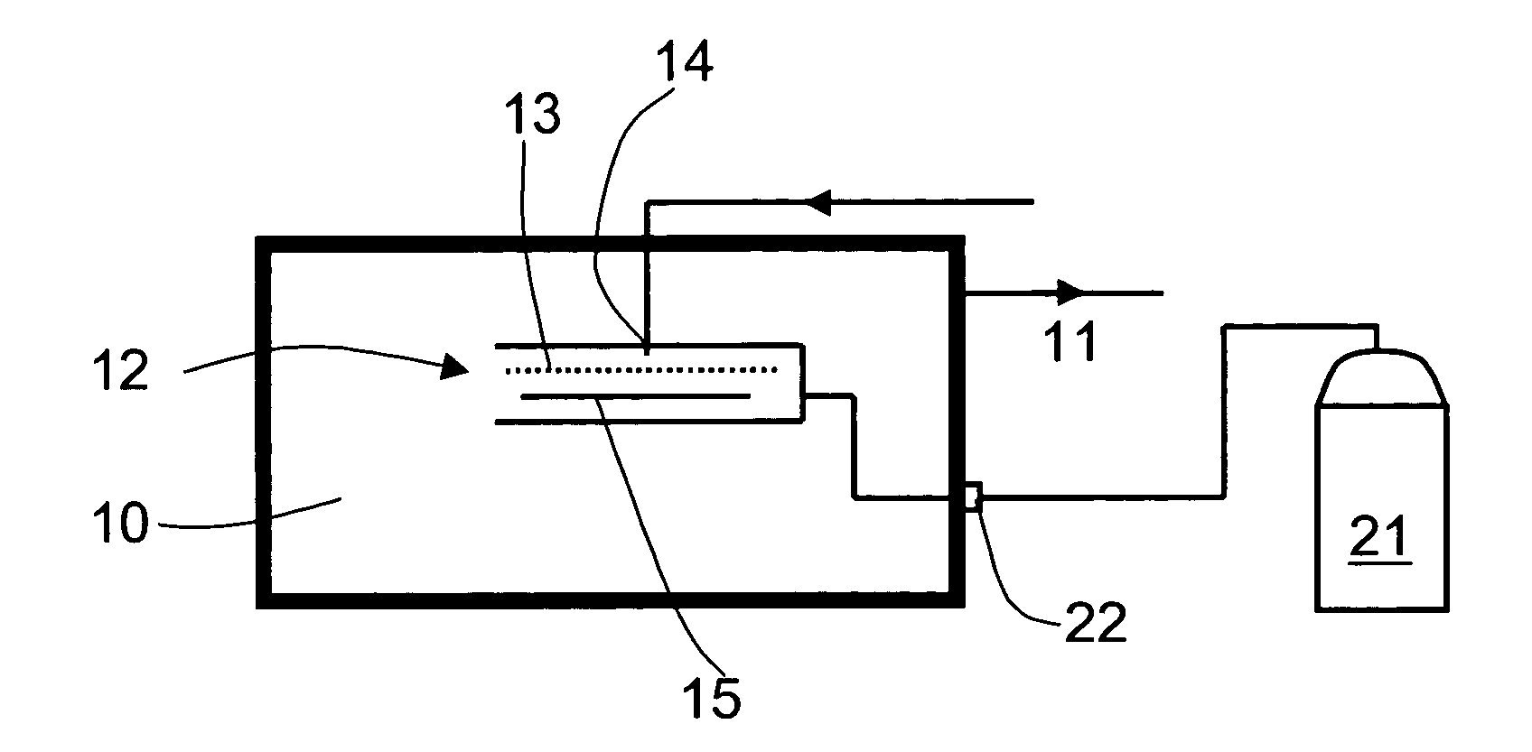
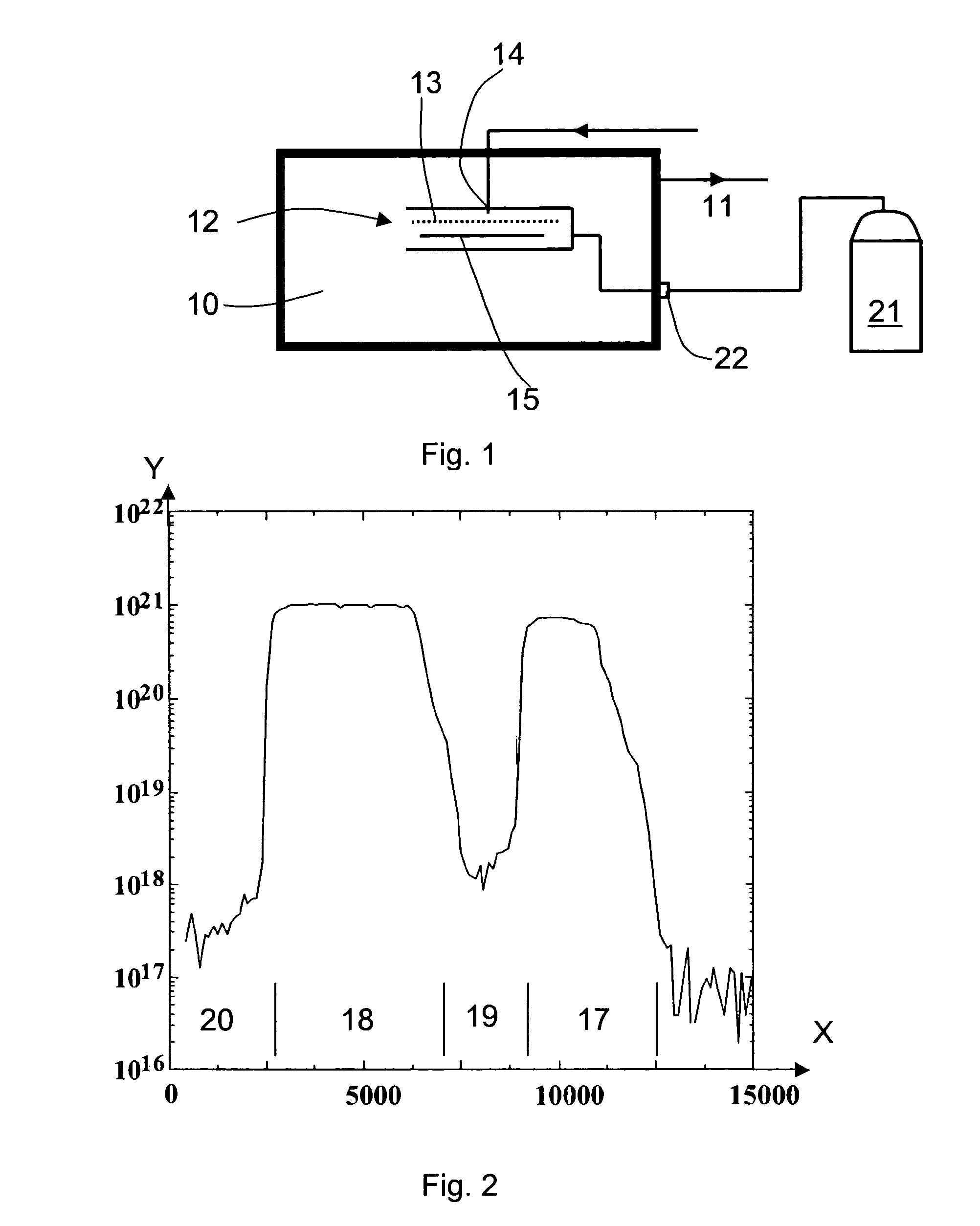
[0038]Therefore, according to the invention, after the deposition of the p-layer and before the deposition of the i-layer, the internal surfaces of the reactor and the substrate also are dosed with a vapour or a gas comprising water, methanol or isopropanol or another alcohol.

[0039]More precisely, in this example, the dosing product is stored in a separate bottle 21 connected, via a valve 22, to the vacuum chamber 10, which is kept at low pressure condition. When the valve 22 is opened, the dosing product starts boiling in the bottle 21 because of the low pressure inside and vapour flushes into the chamber 10. Of- course, the RF electrode 13 is off. The operation is performed between 100 and 350° C., typically at 200° C. and during less than 10 minutes, typically 2 minutes and at 0.05 to 100 mbar. The flow of water vapour has to be sufficient. For example, 90 mbar.sec is a good value. If methanol or isopropanol is used, the flow is generally higher.

[0040]After the dosing operation, ...

second embodiment

[0050]According to the invention, after the deposition of the p-layer and before the deposition of the i-layer, the internal surfaces of the reactor are dosed with a vapour or gas comprising ammonia, hydrazine or volatile organic amines. This dosing operation is performed at low pressure conditions (0.05 to 100 mbar), between 100 and 350° C., typically at around 200° C. and during less than 10 minutes, typically around to 2 minutes. The flow of gas has to be sufficient. For example, 90 mbar.sec is a good value for ammonia. After the dosing operation, a short pumping period of less than 5 minutes is also respected before the deposition of the i-layer.

[0051]A nitrogen peak can be observed with a SIMS analysis at the treated n-i interface, meaning that such a treatment has been used. Typically, the amount of nitrogen is higher than 1019 atoms.cm−3.

[0052]For both embodiments of the invention, it may be useful to depose on the p-layer, after the above described treatments, a hydrogen-dil...


PUM

PropertyMeasurementUnit
Temperatureaaaaaaaaaa
Pressureaaaaaaaaaa

Abstract

A semi-conducting device has at least one layer doped with a doping agent and a layer of another type deposited on the doped layer in a single reaction chamber. An operation for avoiding the contamination of the other layer by the doping agent separates the steps of depositing each of the layers.

Description

BACKGROUND OF THE INVENTION[0001]The present invention relates in general to the domain of semiconductor films based on silicon technology. It concerns, more particularly, a method for producing silicon junctions, doped or not, which can be used, for example, in solar cells. It also concerns any other semi-conducting devices obtained by such a method.[0002]Amorphous or microcrystalline silicon solar cells are made of multilayer systems where semiconducting material with certain electronical and physical properties is deposited, layer by layer, on a substrate.[0003]The n-layers and p-layers are doped with other elements to achieve desired properties, such as electrical conductivity. More precisely:[0004]p-doped layers have a surplus of positive charge carriers,[0005]n-doped layers have a surplus of negative charge carriers, and[0006]i layers are intrinsic.[0007]Generally, boron is used as the doping agent of the p-layers and phosphor as the doping agent of the n-layers.[0008]Silicon ...

Claims


Application Information

Patent Timeline
IPC IPC(8): H01L21/20C23C16/44C23C16/455H01L21/205H01L21/22H01L31/0288H01L31/075H01L31/18H01L31/20
CPCH01L21/0242H01L21/02491H01L21/02529H01L21/02579H01L21/0262H01L21/02664H01L21/2205H01L31/0288H01L31/075H01L31/1804H01L31/202Y02E10/548Y02E10/547Y02P70/50H01L21/20
Inventor KROLL, ULRICHBUCHER, CEDRICSCHMITT, JACQUESPOPPELLER, MARKUSHOLLENSTEIN, CHRISTOPHBALLUTAUD, JULIETTEHOWLING, ALAN
Owner OERLIKON SOLAR AG (TRUEBBACH)
Why Eureka
Try Eureka