
Liquid crystal display device and method of fabricating the same

a display device and liquid crystal technology, applied in non-linear optics, instruments, optics, etc., can solve the problems of affecting the appearance of the liquid crystal display device, so as to facilitate the hardening of the photo-hardening sealant and increase the size of the substrate

Inactive Publication Date: 2008-03-25
LG DISPLAY CO LTD
View PDF246 Cites 7 Cited by
  • Summary
  • Abstract
  • Description
  • Claims
  • Application Information

AI Technical Summary

Benefits of technology

This method ensures complete hardening of the photo-hardening sealant, maintaining adhesion and preventing misalignment, while keeping the substrate size unchanged.

Problems solved by technology

When a wide-screen liquid crystal display is fabricated by a liquid crystal injection method, it takes too much time.
Hence, the photo-hardening sealant 110 cannot be hardened by the UV-ray, thereby weakening the adhesion.
However, the related art liquid crystal display device and the method of fabricating the same have the following problems or disadvantages.
Furthermore, when the UV-ray is applied from the upper side of the substrate, either a pattern of the black matrix layer is modified or the size of the substrate is increased, thereby misaligning the sealant from the black matrix layer.

Method used


Image

  • Liquid crystal display device and method of fabricating the same
  • Liquid crystal display device and method of fabricating the same
  • Liquid crystal display device and method of fabricating the same

Examples


Embodiment Construction

[0047]Reference will now be made in detail to the illustrated embodiments of the present invention, examples of which are illustrated in the accompanying drawings. Wherever possible, the same reference numbers will be used throughout the drawings to refer to the same or like parts.

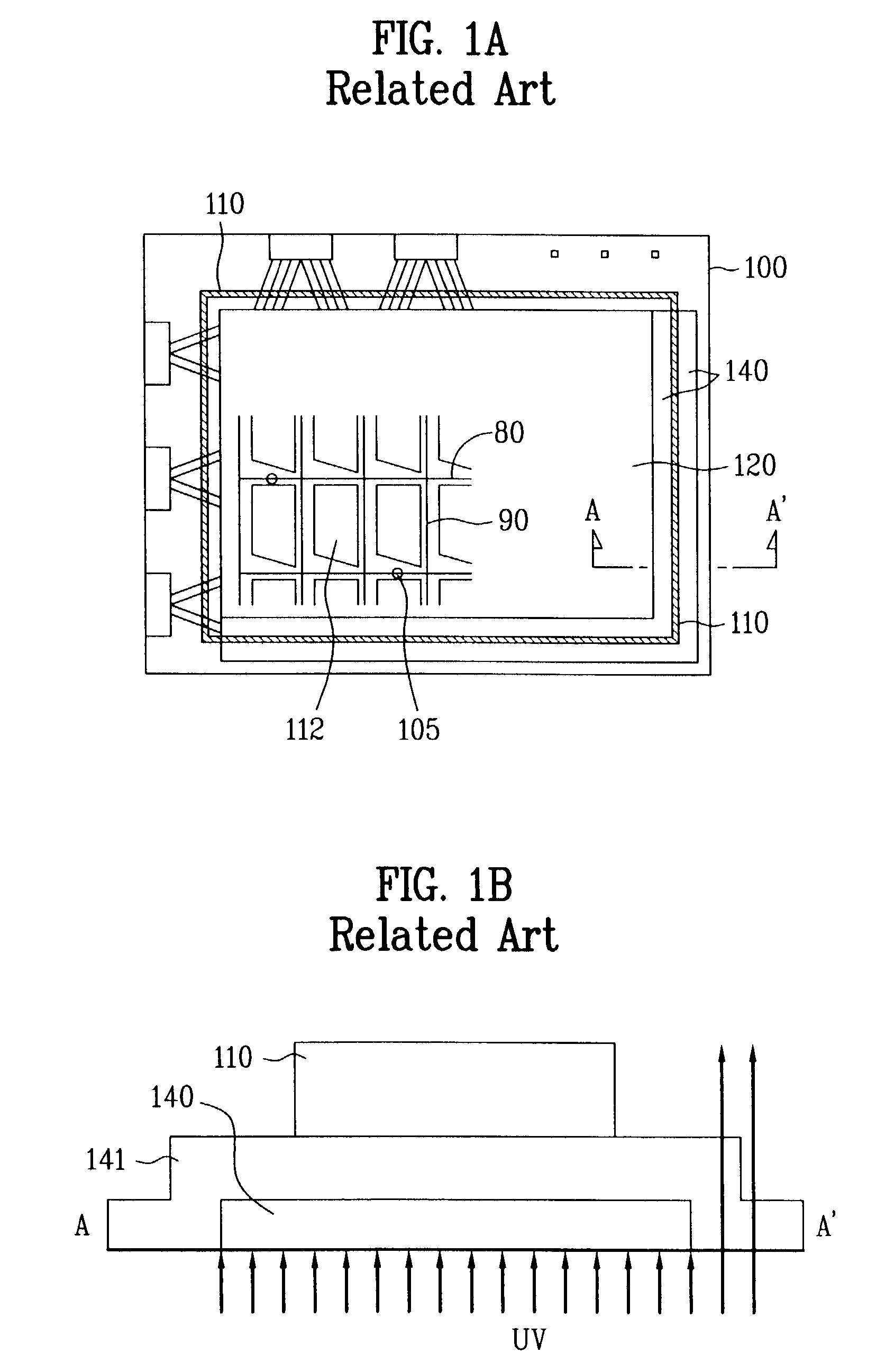
[0048]FIG. 3 illustrates a cross-sectional view of a TN type liquid crystal display device according to the present invention.

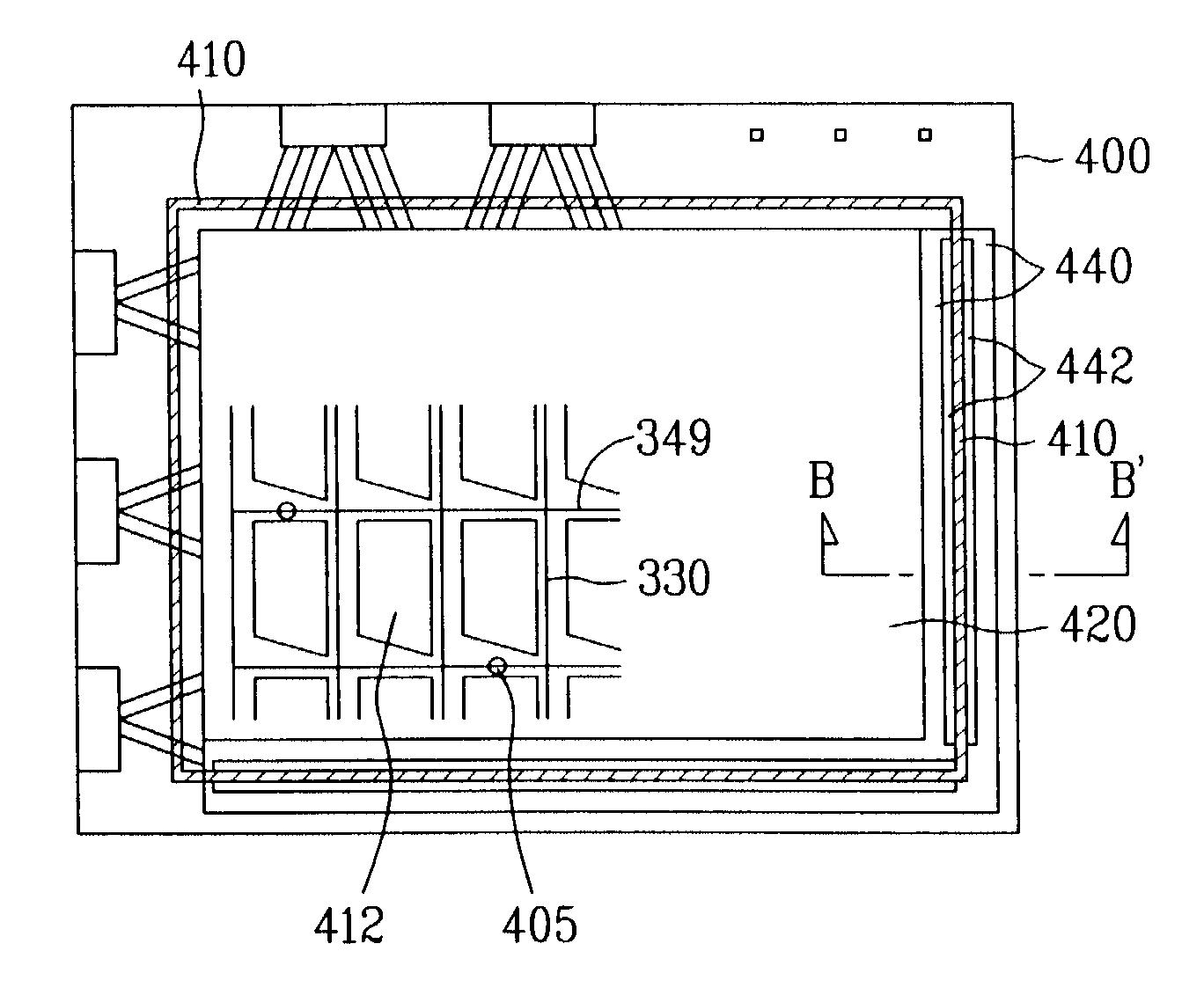
[0049]As shown in FIG. 3, a gate line 349, a gate electrode 309, and a common line 440 of a thin film transistor are formed on a first substrate 300. A gate insulating layer 320 is formed on the entire surface of the first substrate 300. The common line 440 supplies a common electrode with a common voltage and provides a UV-ray irradiation path through which UV-ray is applied to harden a sealant.

[0050]A semiconductor layer 315 is formed on the gate insulating layer 320 over the gate electrode 309. A data line 330 having source and drain electrodes 316 and 317 is formed at both sides...


PUM

PropertyMeasurementUnit
sizeaaaaaaaaaa
pixel areasaaaaaaaaaa
circumferenceaaaaaaaaaa

Abstract

A liquid crystal display device and a method of fabricating the same are disclosed in the present invention. The liquid crystal display device includes a first substrate having a thin film transistor array and a common line with a UV-ray irradiation path passing UV-rays, a second substrate having a color filter array, a sealant between the first and second substrates over the common line, and a liquid crystal layer between the first and second substrates.

Description

[0001]This application claims the benefit of the Korean Patent Application No. P2001-083219 filed on Dec. 22, 2001, which is hereby incorporated by reference.BACKGROUND OF THE INVENTION[0002]1. Field of the Invention[0003]The present invention relates to a display device, and more particularly, to a liquid crystal display device and a method of fabricating the same. Although the present invention is suitable for a wide scope of applications, it is particularly suitable for facilitating hardening of a photo-hardening sealant without modifying a black matrix layer pattern or increasing a size of the substrate.[0004]2. Discussion of the Related Art[0005]Generally, a liquid crystal display device has characteristics, such as low-voltage driving, low power consumption, full-color implementation, thin and compact size, and the like. Thus, it has been widely used for calculators, notebook computers, electronic watches, computer monitors, aircraft gauges, personal mobile terminals, and mobi...

Claims


Application Information

Patent Timeline
Patent Type & Authority Patents(United States)
IPC IPC(8): G02F1/1339G02F1/1362
CPCG02F1/1339G02F2001/13415G02F2001/136295G02F1/13415G02F1/136295
Inventor KIMKANG, SUNG CHUNHA, YOUNG HUN
Owner LG DISPLAY CO LTD
Learn More