

Semiconductor light emitting devices and methods
a technology of semiconductors and light emitting devices, applied in semiconductor devices, lasers, semiconductor lasers, etc., can solve the problems of fundamental limitations of bipolar transistor speed, spontaneous emission recombination lifetime, etc., to promote carrier transport unidirectionally, light emission and device speed are both enhanced, and the directionality and speed of carrier transport is improved
- Summary
- Abstract
- Description
- Claims
- Application Information
AI Technical Summary
Benefits of technology
Problems solved by technology
Method used
Image

Examples
Embodiment Construction
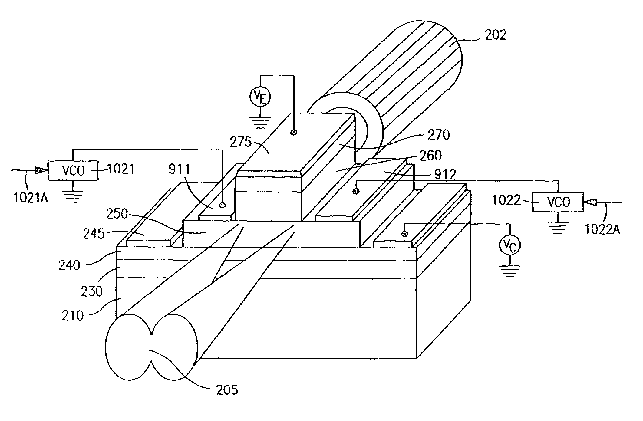
[0030]FIG. 1 illustrates a device as described in the referenced prior applications. A substrate 105 is provided, and the following layers are disposed thereon: subcollector 110, collector 130, base 140, emitter 150, and cap layer 160. Also shown are collector metallization (or electrode) 115, base metallization 145, and emitter metallization 165. Collector lead 117, base lead 147, and emitter lead 167 are also shown. In a described form of this device, the layers were grown by MOCVD, and the collector layer 130 comprised 3000 Angstrom thick n-type GaAs, n=2×1016 cm−3, the base layer 140 comprised 600 Angstrom thick p+ carbon-doped compositionally graded InGaAs (1.4% In), p=4.5×1019 cm−3, the emitter layer 150 comprised 800 Angstrom thick n-type InGaP, n=5×1017 cm−3, and the cap layer comprised 1000 Angstrom thick n+ InGaAs, n=3×1019 cm−3.
[0031]The fabrication process sequence included e-beam defined Ti / Pt / Au emitter contacts (165), a self-aligned emitter etch, a self-aligned Ti / Pt / ...
PUM
 Abstract
Description
Claims
Application Information