Plasma display device with grounding module

a technology of display device and grounding module, which is applied in the direction of identification means, instruments, and connection contact material, etc., can solve the problems of excessive heat buildup, weak mechanical strength of pdp, and inability to resist damage, so as to simplify the mounting and grounding of pbas and enhance the grounding of a pba

Inactive Publication Date: 2008-04-15
SAMSUNG SDI CO LTD
View PDF10 Cites 28 Cited by
  • Summary
  • Abstract
  • Description
  • Claims
  • Application Information

AI Technical Summary

Benefits of technology

[0012]The present invention is therefore directed to a plasma display device having a simplified chassis base structure and enhanced grounding of a PBA, which substantially overcomes one or more of the problems due to the limitations and disadvantages of the related art.
[0013]It is feature of an embodiment of the present invention to provide a plasma display device that combines a chassis base structure with enhanced grounding of a PBA.
[0014]It is another feature of an embodiment of the present invention to provide a plasma display device whereby mounting and grounding of PBAs is simplified.
[0015]It is yet another feature of an embodiment of the present invention to provide a plasma display device whereby grounding of PBAs is not degraded by loosened fasteners.

Problems solved by technology

Generally, the PDP exhibits weak mechanical strength and is susceptible to damage from physical impact.
PDPs also produce substantial amounts of heat during operation and can suffer from excessive heat buildup.
However, the fastening force from the fasteners may cause distortion of the grounding sections of the PBAs, particularly those having a multi-layer structure.
In particular, the construction and materials of the PBAs is not optimal with respect to the amount of compressive force that can be applied thereto.
As a result, torquing the fasteners to the predetermined torque may cause an inelastic deformation of the PBAs in the grounding section, permanently distorting them.
Such distortion of the grounding section may cause a thermal distortion of the PBA as a result of the heat produced during an operation of the PDP, thereby causing fasteners to become unfastened from the fastening hole over time.
Further, the inelastic deformation of the PBAs may result in insufficient tension on the fasteners, thereby causing the fasteners to become unfastened.
As a result, the grounding of the PBA may deteriorate, and, accordingly, the EMI may be increased.

Method used


Image

  • Plasma display device with grounding module
  • Plasma display device with grounding module
  • Plasma display device with grounding module

Examples


second embodiment

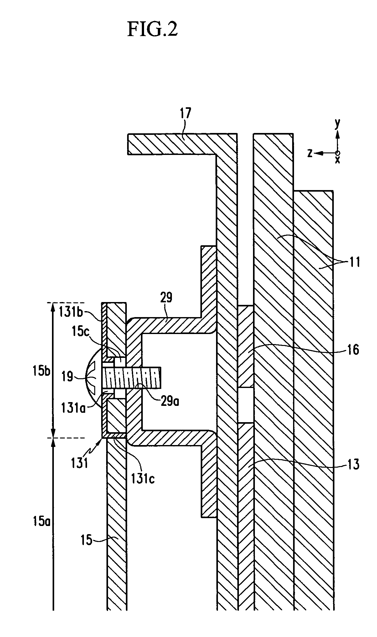
[0050]FIG. 4 illustrates a perspective view of a second embodiment of a grounding module according to the present invention, and FIG. 5 illustrates a partial, sectional view of a plasma display device including the grounding module illustrated in FIG. 4, taken along a line corresponding to line II-II of FIG. 1. Referring to FIGS. 4 and 5, in accordance with a second embodiment of the grounding module 131 of the present invention, a pair of first and second grounding modules 231 and 232 may be provided. The first grounding module 231 may be provided for the fastening hole 15c on one side of the grounding section 15b of the PBA 15. The second grounding module 232 may be provided for the fastening hole 15c on the other side of the grounding section 15b of the PBA 15.

[0051]The first and second grounding modules 231 and 232 may be disposed symmetrically, and on both sides of the grounding section 15b of the PBA 15. The first and second grounding modules 231 and 232 may be in physical and...

third embodiment

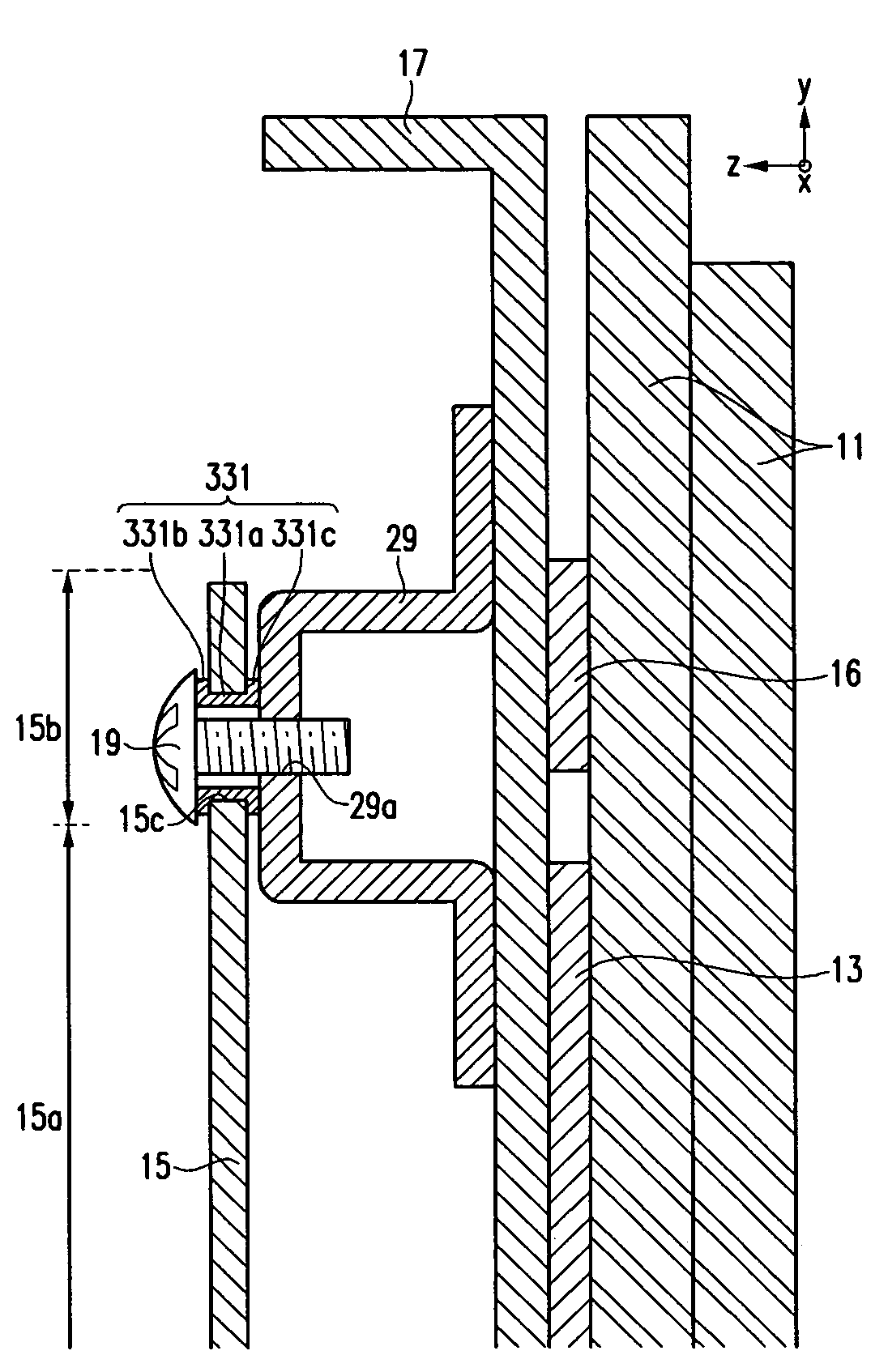
[0054]FIG. 6 illustrates a perspective view of a third embodiment of a grounding module according to the present invention, and FIG. 7 illustrates a partial, sectional view of a plasma display device including the grounding module illustrated in FIG. 6, taken along a line corresponding to line II-II of FIG. 1. Referring to FIGS. 6 and 7, a grounding module 331 according to a third embodiment may include a cylinder 331a and flanges 331b and 331c. The cylinder 331a may be inserted into the fastening hole 15c. The flanges 331b and 331c may formed by bending opposite ends of the cylinder 331a in a radial direction such that the flanges 331b and331c make electrical contact with the grounding section 15b around the peripheral area of the fastening hole 15c on both sides of the grounding section 15b of PBA 15. Alternatively, the grounding module 331 may include the cylinder 331a and only one of the two flanges 331b and 331c (not shown).

[0055]The flanges 331b and 331c provided on opposing e...

fourth embodiment

[0056]FIG. 8 illustrates a perspective view of a fourth embodiment of a grounding module according to the present invention, and FIG. 9 illustrates a partial, sectional view of a plasma display device including the grounding module illustrated in FIG. 8, taken along a line corresponding to line II-II of FIG. 1. Referring to the FIGS. 8 and 9, a grounding module 431 according to a fourth embodiment of the present invention may include a circular flange 431a, first and second base plates 431b and 431e, and a lateral connection portion 431c. The circular flange 431a may be inserted into the fastening hole 15c. The first base plate 431b may be planarly formed around the circular flange 431a so as to contact the grounding section 15b. The lateral connection portion 431c may be formed by bending the first base plate 431b. The second base plate 431e may be formed by bending the lateral connection portion 431c such that it is parallel to the first base plate 431b. A penetration hole 431d ma...


PUM


Abstract

A plasma display device includes a plasma display panel mounted on a first side of a chassis base, a mount on a second side of the chassis base, the mount being electrically connected to the chassis base, a printed circuit board including an electrical grounding section and having an opening in the electrical grounding section, the printed circuit board mounted on the mount by an electrically conductive fastener passing through the opening in the electrical grounding section, and a grounding module positioned in the opening so as to be between the electrical grounding section and the electrically conductive fastener and electrically connecting the electrical grounding section to the mount.

Description

BACKGROUND OF THE INVENTION[0001]1. Field of the Invention[0002]The present invention relates to a plasma display device. More particularly, the present invention relates to a plasma display device having a simplified chassis base structure and a grounding module for enhancing grounding of a printed circuit board assembly.[0003]2. Description of the Related Art[0004]A plasma display device is an apparatus that displays an image from a plasma display panel (PDP) using plasma generated by a gas discharge. Typically, the plasma display device includes the PDP, a chassis base supporting the PDP, and a plurality of printed circuit board assemblies (PBAs) mounted to the chassis base on a side opposite of the PDP. The PBAs may be connected to display electrodes or address electrodes via, e.g., flexible printed circuits (FPCs) and connectors.[0005]A typical PDP includes two glass substrates attached to each other at peripheral regions of their surfaces with a discharge space formed therebet...

Claims


Application Information

Patent Timeline
Patent Type & Authority Patents(United States)
IPC IPC(8): H01R12/00G09F9/00H05K7/14
CPCH05K7/142H05K9/0039H01R4/34H01R4/64H01J11/34
Inventor JEONG, JAE-SEOKKANG, TAE-KYOUNG
Owner SAMSUNG SDI CO LTD
Why Eureka
Try Eureka