Defect reduction of non-polar and semi-polar III-Nitrides with sidewall lateral epitaxial overgrowth (SLEO)

a technology of non-polar and semi-polar iiinitrides and epitaxial overgrowth, which is applied in the direction of basic electric elements, electrical apparatus, and semiconductor devices, can solve the problems of gan materials that perform poorly, devices that perform poorly, and reduce the likelihood, so as to eliminate polarization fields, reduce dislocation density, and prolong life

Active Publication Date: 2008-04-22
JAPAN SCI & TECH CORP
View PDF53 Cites 121 Cited by
  • Summary
  • Abstract
  • Description
  • Claims
  • Application Information

AI Technical Summary

Benefits of technology

[0017]The general purpose of the present invention is to create high quality (minimum defect density) non-polar a-{11-20} and m-{1-100} plane and semi-polar {10-1n} plane III-Nitride material by employing lateral overgrowth from sidewalls of etched nitride material through a dielectric mask. The method includes depositing a patterned mask on non-polar or semi-polar III-Nitride template, etching the template material down to various depths through openings in the mask, and regrowing the non-polar or semi-polar epitaxial film by coalescing laterally from the tops of the sidewalls before the vertically growing material from the trench bottoms reaches the surface. The coalesced features grow through the openings of the mask, and grow laterally over the dielectric mask until a fully coalesced continuous film is achieved.
[0018]These planar non-polar materials grown heteroepitaxially, such as a-GaN on top of r-Al2O3, contain dislocation densities of ˜1010 cm−2 and stacking fault densities of 3.8×105 cm−1 (aligned perpendicular to the c-axis) throughout the film. By using single step lateral epitaxial overgrowth, dislocation densities can be reduced down to ˜107-109 cm−2 and stacking faults are localized only on the nitrogen faces. With the present invention, using sidewall lateral epitaxial overgrowth, dislocation densities can be reduced down to even lower values by eliminating defects not only in the overgrown regions but also in the window regions. Also, by favoring gallium (Ga) face growth and limiting nitrogen (N) face growth stacking fault densities can be made orders of magnitude lower.
[0019]The present invention also takes advantage of the orientation of non-polar III-Nitrides to eliminate polarization fields. As a result, with the material produced by utilizing this invention, device improvements such as longer lifetimes, less leakage current, more efficient doping and higher output efficiency will be possible. In addition, a thick non-polar and semi-polar nitride free-standing substrate, which is needed to solve the lattice mismatch issue, can be produced over this excellent material by various methods.

Problems solved by technology

However, as a result of c-plane growth, each material layer suffers from separation of electrons and holes to opposite faces of the layers.
Such polarization effects decrease the likelihood of electrons and holes recombining, causing the device to perform poorly.
Another reason why GaN materials perform poorly is the presence of defects due to lack of a lattice matched substrate.
Bulk crystals of GaN are not widely available so it is not possible to simply cut a crystal to present a surface for subsequent device regrowth.
The two predominant types of extended defects of concern are threading dislocations and stacking faults.

Method used


Image

  • Defect reduction of non-polar and semi-polar III-Nitrides with sidewall lateral epitaxial overgrowth (SLEO)
  • Defect reduction of non-polar and semi-polar III-Nitrides with sidewall lateral epitaxial overgrowth (SLEO)
  • Defect reduction of non-polar and semi-polar III-Nitrides with sidewall lateral epitaxial overgrowth (SLEO)

Examples


Embodiment Construction

[0027]In the following description of the preferred embodiment, reference is made to the accompanying drawings that form a part hereof, and in which is shown by way of illustration a specific embodiment in which the invention may be practiced. It is to be understood that other embodiments may be utilized and structural changes may be made without departing from the scope of the present invention.

[0028]Overview

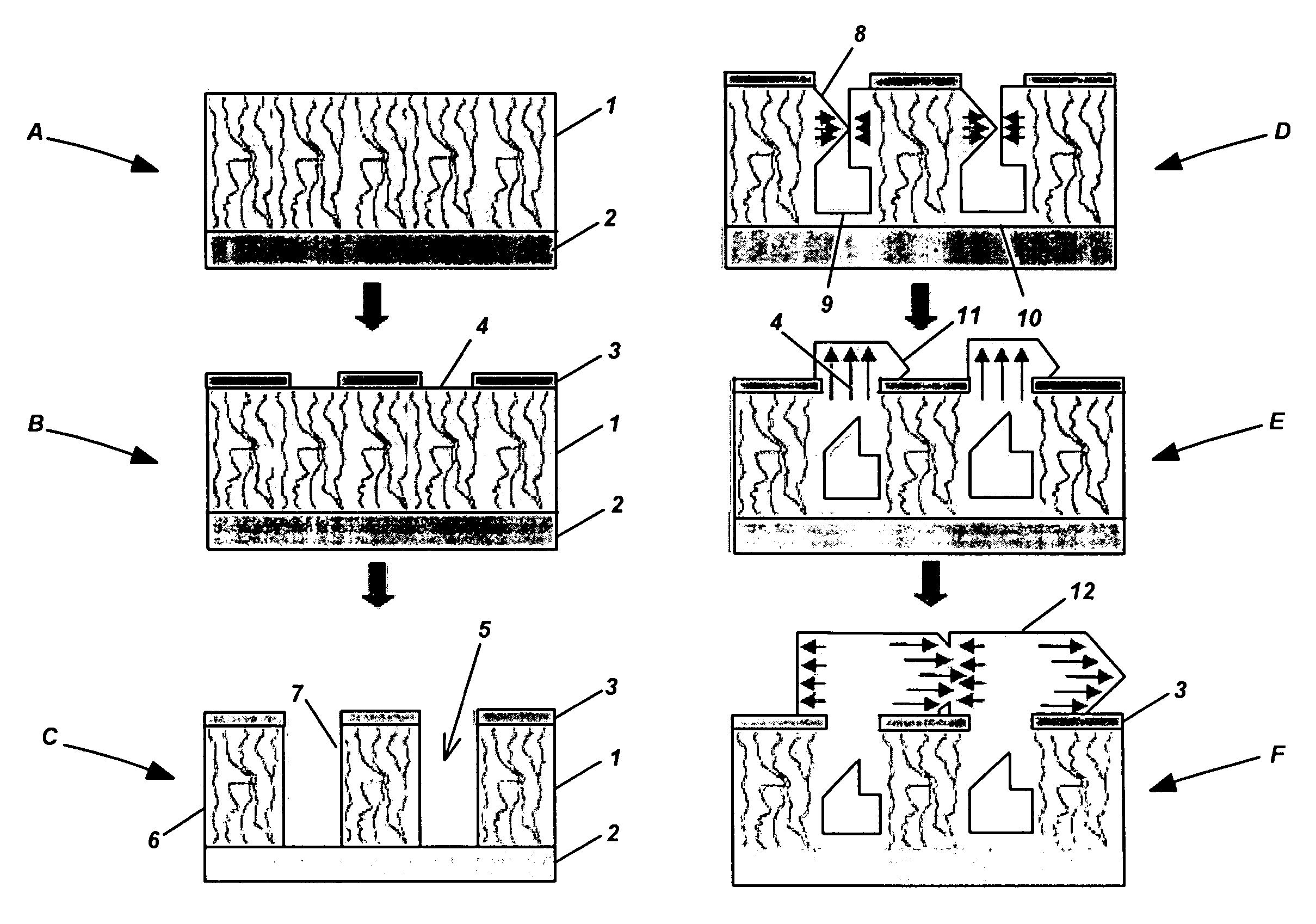
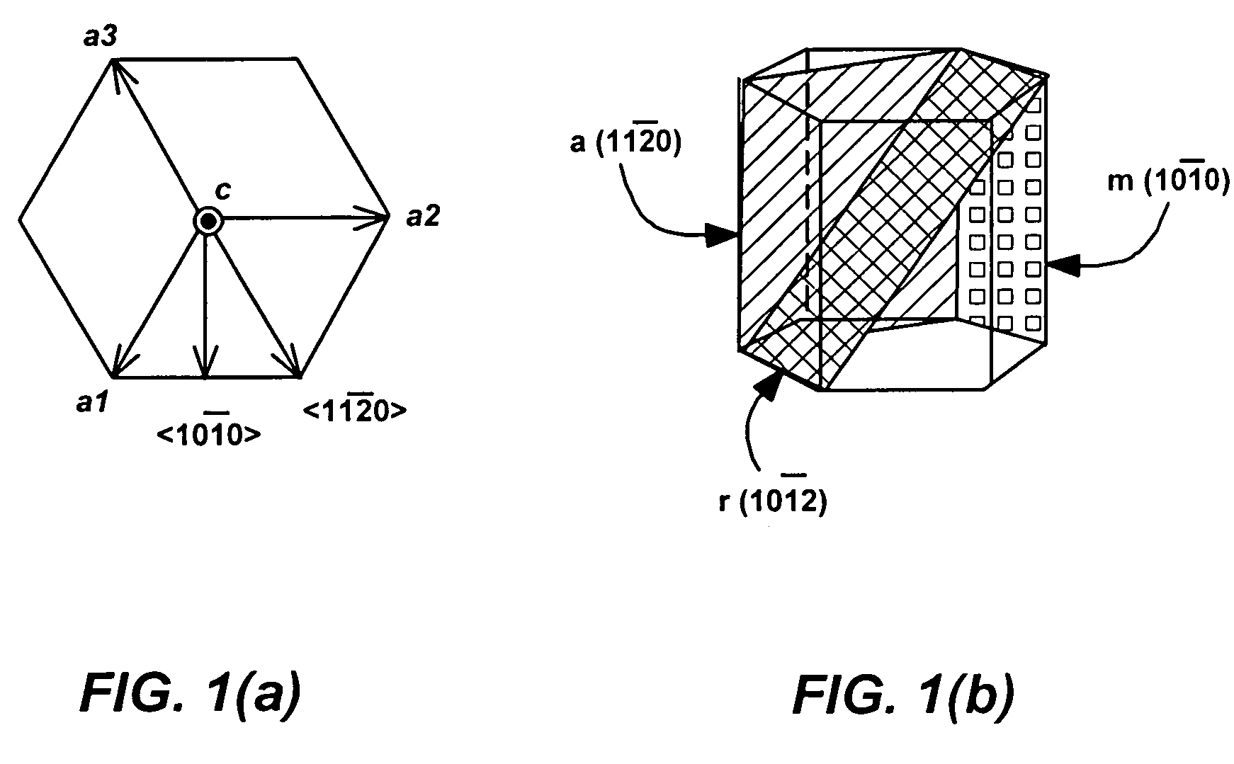
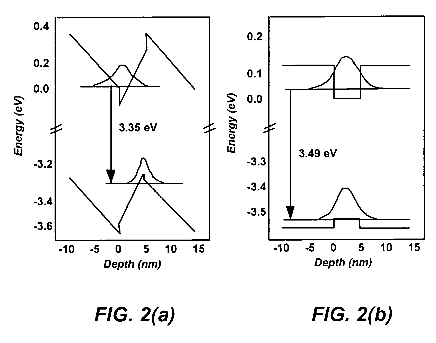
[0029]The growth of (Ga, In, Al, B)N materials in the polar [0001] c-direction causes lower performance in optical devices due to polarization fields causing charge separation along the primary conduction direction. Therefore, research has recently been conducted on non-polar direction growth along the a-[11-20] and m-[1-100] directions of these materials to eliminate such effects and improve device performance significantly.

[0030]Another problem that is common to polar, semi-polar and non-polar III-Nitride materials is high defect densities, the most common of which are disloc...


PUM


Abstract

A method of reducing threading dislocation densities in non-polar such as a-{11-20} plane and m-{1-100} plane or semi-polar such as {10-1n} plane III-Nitrides by employing lateral epitaxial overgrowth from sidewalls of etched template material through a patterned mask. The method includes depositing a patterned mask on a template material such as a non-polar or semi polar GaN template, etching the template material down to various depths through openings in the mask, and growing non-polar or semi-polar III-Nitride by coalescing laterally from the tops of the sidewalls before the vertically growing material from the trench bottoms reaches the tops of the sidewalls. The coalesced features grow through the openings of the mask, and grow laterally over the dielectric mask until a fully coalesced continuous film is achieved.

Description

CROSS-REFERENCE TO RELATED APPLICATIONS[0001]This application claims the benefit under 35 U.S.C. Section 119(e) of the following co-pending and commonly-assigned U.S. patent application:[0002]U.S. Provisional Patent Application Ser. No. 60 / 685,952, filed on May 31, 2005, by Bilge M. Imer, James S. Speck and Steven P. Denbaars, entitled “DEFECT REDUCTION OF NON-POLAR GALLIUM NITRIDE WITH SINGLE-STEP SIDEWALL LATERAL EPITAXIAL OVERGROWTH”;[0003]which application is incorporated by reference herein.[0004]This application is related to the following co-pending and commonly-assigned applications:[0005]U.S. patent application Ser. No. 11 / 444,083, filed on May 31, 2006, by Bilge M. Imer, James S. Speck and Steven P. DenBaars, entitled “GROWTH OF PLANAR NON-POLAR {1-100} M-PLANE GALLIUM NITRIDE WITH METALORGANIC CHEMICAL VAPOR DEPOSITION (MOCVD),” (2005-566), which application claims the benefit under 35 U.S.C. Section 119(e) of U.S. Provisional Patent Application Ser. No. 60 / 685,908, filed...

Claims


Application Information

Patent Timeline
Patent Type & Authority Patents(United States)
IPC IPC(8): H01L21/20H01L21/36H01L33/32
CPCH01L21/0242H01L21/02433H01L21/02458H01L21/02516H01L21/0265H01L21/02609H01L21/0262H01L21/02639H01L21/02647H01L21/0254H01L21/20
Inventor IMER, BILGE M.SPECK, JAMES S.DENBAARS, STEVEN P.
Owner JAPAN SCI & TECH CORP
Why Eureka
Try Eureka