Semiconductor device-based sensors

a technology of semiconductors and sensors, applied in biochemistry, instruments, enzymology, etc., can solve problems such as change in drain curren

Inactive Publication Date: 2008-04-22
MACOM TECH SOLUTIONS HLDG INC
View PDF104 Cites 110 Cited by
  • Summary
  • Abstract
  • Description
  • Claims
  • Application Information

AI Technical Summary

Problems solved by technology

This adsorption may lead to a change in drain current.

Method used


Image

  • Semiconductor device-based sensors
  • Semiconductor device-based sensors
  • Semiconductor device-based sensors

Examples


Embodiment Construction

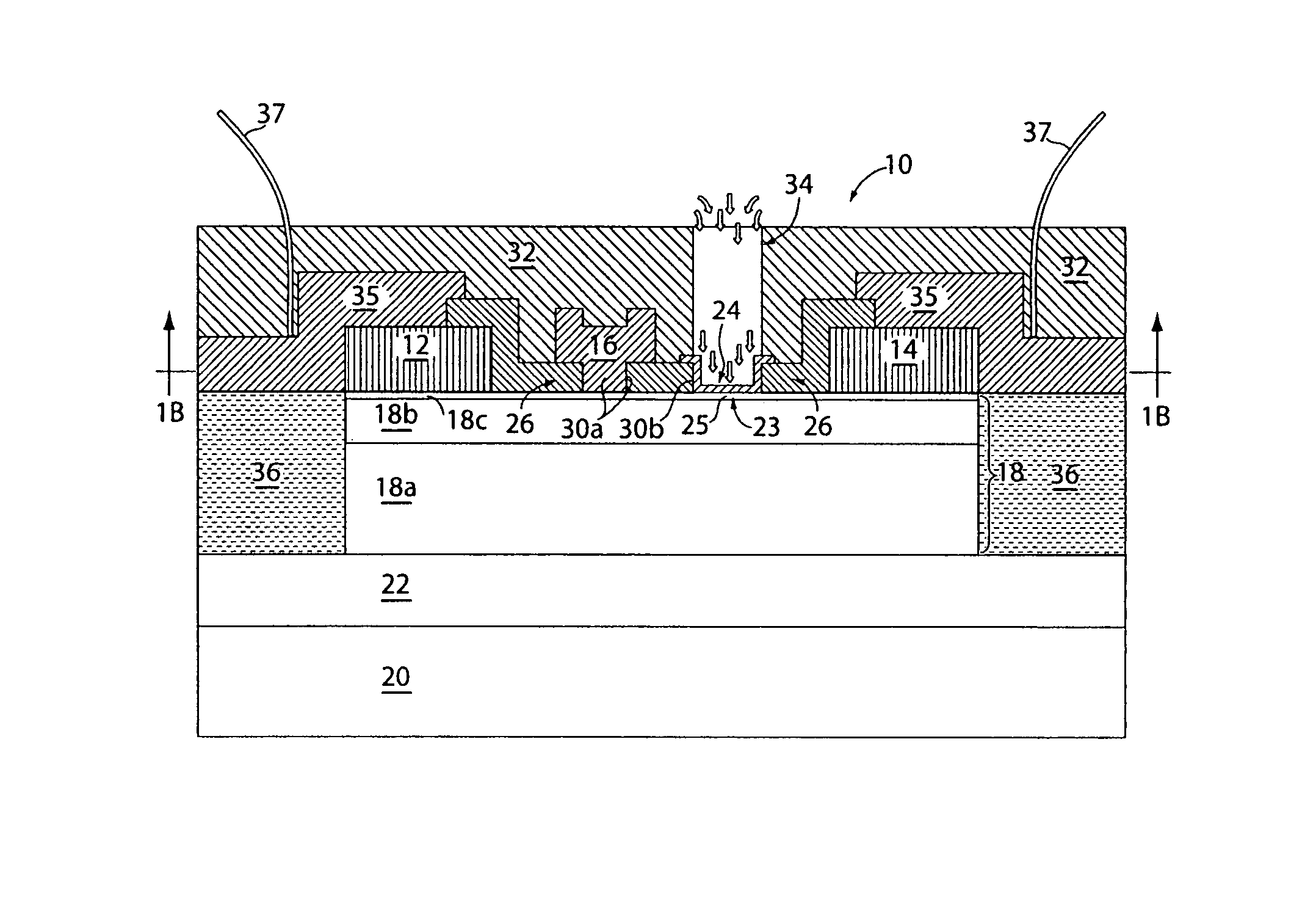
[0020]The invention provides semiconductor device-based chemical sensors and methods associated with the same. The sensors include a sensing region that can interact with chemical species being detected. The chemical species may, for example, be a component of a fluid (e.g., gas or liquid). The interaction between the chemical species and a region of the sensor causes a change in a measurable property (e.g., an electrical property such as drain current) of the device. These changes may be related to the concentration of the chemical species in the medium being characterized. As described further below, the sensing region may be the combination of a sensing layer (e.g., a sensing electrode) and an underlying semiconductor material region, or an exposed semiconductor material (e.g., gallium nitride material) region. Sensors of the invention may be used in a wide variety of applications including engine emission monitoring, carbon dioxide detection and flue gas monitoring, amongst othe...


PUM

PropertyMeasurementUnit
thicknessaaaaaaaaaa
thicknessaaaaaaaaaa
thicknessaaaaaaaaaa

Abstract

Semiconductor device-based chemical sensors and methods associated with the same are provided. The sensors include regions that can interact with chemical species being detected. The chemical species may, for example, be a component of a fluid (e.g., gas or liquid). The interaction between the chemical species and a region of the sensor causes a change in a measurable property (e.g., an electrical property) of the device. These changes may be related to the concentration of the chemical species in the medium being characterized.

Description

BACKGROUND OF INVENTION[0001]The invention relates generally to semiconductor device-based sensors and, more particularly, to gallium nitride material-based transistors that function as chemical sensors and methods associated with the same.[0002]Sensors may be used in many applications, for example, to detect the concentration of a chemical species. The chemical species may be a component of a fluid (e.g., a gas or a liquid) to which the sensor is exposed.[0003]Semiconductor devices have been used as chemical sensors. For example, field effect transistor-based sensors may detect the concentration of a chemical species by measuring changes in drain current (i.e., source-to-drain current) that result from adsorption of the chemical species on the surface of the gate electrode. This adsorption may lead to a change in drain current. The change in the drain current may be related to the concentration of the adsorbed chemical species which, in turn, may be related to the concentration of ...

Claims


Application Information

Patent Timeline
Patent Type & Authority Patents(United States)
IPC IPC(8): H01L23/58G01N27/414H01L21/00
CPCG01N27/129G01N27/414H01L2224/48091G01N27/4148H01L2924/00014
Inventor JOHNSON, JERRY W.PINER, EDWIN L.LINTHICUM, KEVIN J.
Owner MACOM TECH SOLUTIONS HLDG INC
Why Eureka
Try Eureka