Semiconductor device and semiconductor assembly module with a gap-controlling lead structure

Active Publication Date: 2008-04-22
MITSUBISHI ELECTRIC CORP
View PDF39 Cites 34 Cited by
  • Summary
  • Abstract
  • Description
  • Claims
  • Application Information

AI Technical Summary

Benefits of technology

[0021]In the semiconductor device, the temperature rise property of the leads is improved due to increase of the heat resistance of the heat-release path extending from the leads to the plastic package and the solderability is improved. Moreover, because the first lead portion has a large stiffness, the easiness of fabrication of the

Problems solved by technology

Therefore, because the temperature of the portion B1 of the lead 104 which should be soldered does not reach the liquidus-line temperature of solder under the soldering process, a problem occurs that imperfect soldering is made.
This is because it is difficult to raise a process temperature such as a preheating temperature or melted-solder temperature in order to compensate the rise value (40° K.) of the liquidus-line temperature of solder.
However, the above method has a problem that the solderability is not improved at all in the case of the lead 207 whose lead step portion 211 is closest to a substrate.
In this point, it is insufficient to solve the problem by the above method.
Particularly, in the case of solder mount using lead-free solder having a high liquidus-line temperature, there is a problem that imperfect soldering may frequency occur.
Therefore, to form two or more lead-step portions on same-height places, there is a problem that the design of the leads must be greatly restricted.
However, when forming the lead-step portions on the same-height places between the metallic leads having volumes different from each other at the lead-embedding portion, there is a problem that preferable solderability may not be secured.
Moreover, there is a problem that it is very complicated to decide the

Method used


Image

  • Semiconductor device and semiconductor assembly module with a gap-controlling lead structure
  • Semiconductor device and semiconductor assembly module with a gap-controlling lead structure
  • Semiconductor device and semiconductor assembly module with a gap-controlling lead structure

Examples


Example

Embodiment 1

[0049]The embodiment 1 of the present invention will be described below. The semiconductor device of the embodiment 1 is a package-type large DIP corresponding to static electricity.

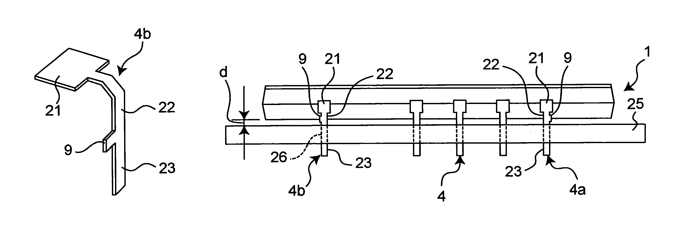
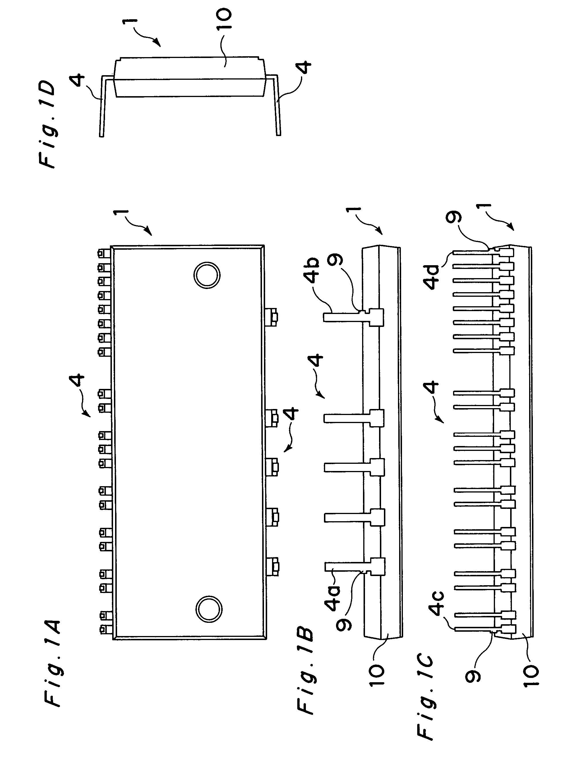
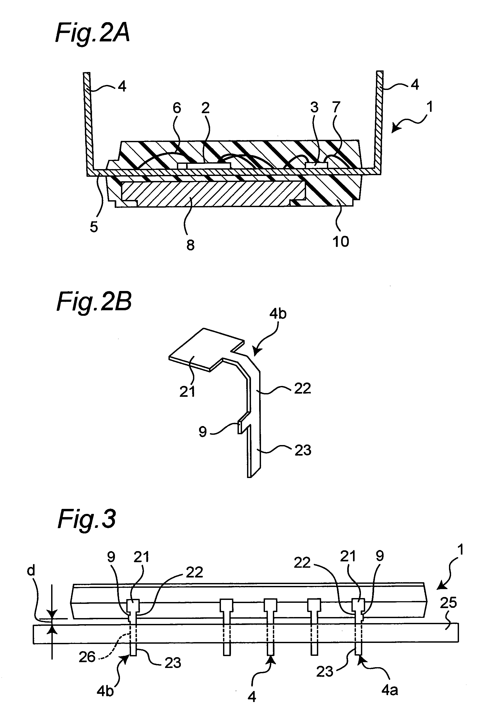
[0050]FIGS. 1A–1D are a top view, front view, rear view and side view of the semiconductor device of the embodiment 1, respectively. FIG. 2A is a side sectional view of the semiconductor device while FIG. 2B is an enlarged perspective view of one end lead of the semiconductor device. FIG. 3 is a front view showing a state in which the semiconductor device is mounted on a substrate. The semiconductor device shown in FIGS. 1A–1D to FIG. 3 is a so-called semiconductor device of an insertion-mount-type or an insertion-mount-type semiconductor device.

[0051]As shown in FIGS. 1A–1D to FIG. 3, in the semiconductor device of the embodiment 1, a power semiconductor element 2 and a control semiconductor element 3 are mounted on a copper lead frame 5 provided with a plurality of leads 4. Both of the semi...

Example

Embodiment 2

[0071]The embodiment 2 of the present invention will be described below by referring to FIGS. 8A and 8B toFIG. 10. The semiconductor device of the embodiment 2 has many points common to those of the embodiment 1 shown in FIGS. 1A–1D to FIG. 7. Therefore, to avoid duplication of description, points of the embodiment 2 different from those of the embodiment 1 are mainly described below. In FIGS. 8A and 8B to FIG. 10, a member common to that of the embodiment 1 shown in FIGS. 1A–1D to FIG. 7 is provided with the same reference number. Though a case is described below in which the shape of the gap-controlling portion 9 is rectangular, the shape is not restricted to a rectangle. A square, trapezoidal, or triangular shape is allowed as long as the shape can control a gap.

[0072]FIG. 8A is a front view of a semiconductor device of the embodiment 2. FIG. 8B is an enlarged perspective view of an end lead of the semiconductor device. The semiconductor device shown in FIGS. 8A and 8...

Example

Embodiment 3

[0080]The embodiment 3 of the present invention will be described below by referring to FIGS. 11A–11C to FIG. 13. A semiconductor device of the embodiment 3 has many points common to the semiconductor device of the embodiment 1 shown in FIGS. 1A–1D to FIG. 7. Therefore, to avoid duplication of description, points different from those of the embodiment 1 are mainly described below. In FIGS. 11A–11C to FIG. 13, a member common to that of the embodiment 1 shown in FIGS. 1A–1D to FIG. 7 is provided with the same reference number.

[0081]FIG. 11A is a front view of a semiconductor device of the embodiment 3. FIG. 11B is an enlarged perspective view showing one end lead of the semiconductor device. FIG. 11C is a perspective view showing a modification of an end lead. The semiconductor device shown in FIGS. 11A–11C is an insertion-mount-type semiconductor device.

[0082]As shown in FIGS. 11A–11C, in the case of the semiconductor device 1 of the embodiment 3, a gap-controlling porti...


PUM


Abstract

In a semiconductor device (1), semiconductor elements (2) and (3) are mounted on a lead frame (5) having leads (4). The semiconductor elements (2) and (3) are connected with the leads (4) by metallic wires (6) and (7). The semiconductor device (1) also has a heat sink (8). The members (2) to (8) are sealed with a plastic package (10). The leads (4) are exposed outward. Each of the end leads (4a) to (4d) has a wide first lead portion, a narrow second lead portion, a third lead portion to be inserted into an external substrate, and a protruding gap-controlling portion (9) for keeping the gap between the semiconductor device (1) and the external substrate constant. Because the heat resistance from the leads (4) to the plastic package (10) increases, the temperature-rise property of the lead is improved so that the solderability is improved.

Description

BACKGROUND OF THE INVENTION[0001]1. Field of the Invention[0002]The present invention relates to a semiconductor device of an insertion-mount-type and a semiconductor assembly module, more specifically relates to a semiconductor device capable of improving the solderability of leads, particularly improving the solderability of the leads for lead-free solder mounting of a power module and a semiconductor assembly module using the semiconductor device.[0003]2. Description of the Related Art[0004]In general, a semiconductor device of an insertion-mount-type is mounted on an external substrate by inserting leads protruding from the semiconductor device into through-holes of the external substrate. A structure of a conventional semiconductor device of an insertion-mount-type and a method for mounting the semiconductor device on an external substrate are described below by using the DIPIPM shown in FIGS. 23A–23D andFIG. 24 as an example.[0005]As shown in FIGS. 23A–23D and FIG. 24, in the ...

Claims


Application Information

Patent Timeline
IPC IPC(8): H01L23/48H01L23/34H01L23/495H05K3/30H01L23/50H01L23/433
CPCH01L23/49541H01L24/49H05K3/308H01L23/4334H01L23/49575H01L2224/45124H01L2224/45144H01L2224/48091H01L2224/48137H01L2224/48247H01L2224/49H01L2924/01002H01L2924/01004H01L2924/01005H01L2924/01006H01L2924/01013H01L2924/01029H01L2924/01033H01L2924/0105H01L2924/01078H01L2924/01079H01L2924/01082H01L2924/01083H01L2924/01322H01L2924/1815H01L2924/19041H01L2924/19043H01L2924/00014H01L24/45H01L24/48H01L2924/01019H01L2924/01023H01L2924/014H01L2924/15747H01L2924/00H01L2924/181H01L2924/00012H01L23/50
Inventor HAYASHI, KENICHIKAWAFUJI, HISASHIMURAI, JUNICHIIZUTA, GORO
Owner MITSUBISHI ELECTRIC CORP
Why Eureka
Try Eureka