
Device and method for fabricating liquid crystal display device

a liquid crystal display and device technology, applied in the direction of identification means, instruments, controlling lamination, etc., can solve the problems of poor productivity of such inability to research enhancing the picture quality of lcd devices, and inability to fabricate lcd devices using the above related art liquid crystal injection methods, etc., to achieve simplified lcd fabrication process layout, simplified device overall structure, and reduced overall size

Active Publication Date: 2008-04-29
LG DISPLAY CO LTD
View PDF260 Cites 7 Cited by
  • Summary
  • Abstract
  • Description
  • Claims
  • Application Information

AI Technical Summary

Benefits of technology

[0026]An advantage of the present invention provides a substrate bonding device and a method for fabricating LCD panels wherein the overall structure of the device is simplified and the overall size of the device is reduced such that a layout of LCD fabrication processes may be simplified, smooth alignment may be provided between substrates, and a period of time required to fabricate a single LCD panel may be reduced to facilitate the smooth progression of preceding and subsequent LCD fabrication processes.

Problems solved by technology

Despite various technical developments in LCD technology, however, research in enhancing the picture quality of LCD devices has been lacking compared to research in other features and advantages of LCD devices.
Fabricating LCD devices using the aforementioned related art liquid crystal injection method, however, is disadvantageous because the productivity of such liquid crystal injection methods is poor.
Moreover, as the size of the LCD panel increases, the risk of defects within the LCD panel increases due to imperfect filling characteristics of the liquid crystal material.
Further, the liquid crystal injection methods are often complicated, time consuming, and require many liquid crystal injection devices that occupy excessive amounts of space.
Use of the aforementioned related art substrate LCD device substrate bonding device is disadvantageous, however, because the overall size of the aforementioned related art substrate bonding device is excessively large, especially when designed to fabricate large-sized LCD panels.
The excessively large overall size of the related substrate bonding device creates problems when designing LCD device fabrication processes because an adequate amount of space must be provided to install the related art substrate bonding device while preserving the space in which other apparatuses of other processes are located.
Further, while the related art bonding device applies sealant and liquid crystal material to substrates supporting thin film transistors and color filter layers and bonds the two substrates together, the related art bonding device may increases the overall amount of time required to fabricate one LCD panel.
Moreover, the overall productivity of the LCD fabrication process is reduced since the related art substrate bonding device cannot process material transported thereto while other fabrication processes are in progress.
As a result, air may leak from the external environment into the enclosed space defined by the upper and lower chamber units and the substrates may become damaged during bonding, thereby creating a defective bond.
Such alignment can be extremely difficult and complicated and unduly lengthen the entire process of fabricating the LCD panel.

Method used


Image

  • Device and method for fabricating liquid crystal display device
  • Device and method for fabricating liquid crystal display device
  • Device and method for fabricating liquid crystal display device

Examples


Embodiment Construction

[0049]Reference will now be made in detail to embodiments of the present invention, examples of which are illustrated in the accompanying drawings.

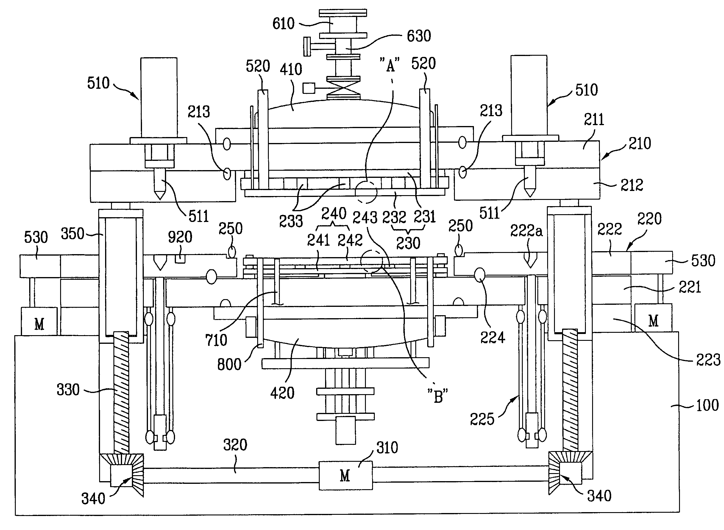
[0050]FIG. 3 illustrates a substrate bonding device for fabricating LCD panels in accordance with the principles of the present invention in an unloaded state.

[0051]Referring to generally to FIG. 3, the substrate bonding device of the present invention may, for example, include a base frame 100; an upper chamber unit 210; a lower chamber unit 220; chamber moving means (e.g., 310, 320, 330, 340, and 350); an upper stage 230; and a lower stage 240; sealing means (e.g., 250); an upper low vacuum unit 410; a lower low vacuum unit 420; alignment means (e.g., 510, 520, 530, and 540) shown, for example, in FIG. 5, vacuum pumping means (e.g., 610, 621, and 622) shown, for example, in FIG. 6; support means (e.g., 710 and 720), shown for example, in FIG. 7; and photosetting means 800.

[0052]In one aspect of the present invention, the base frame 100 ...


PUM

PropertyMeasurementUnit
sizeaaaaaaaaaa
sizeaaaaaaaaaa
distanceaaaaaaaaaa

Abstract

A device for fabricating LCD devices includes a base frame, a lower chamber unit on the base frame, an upper chamber unit over the lower chamber unit and moveable over the base frame, chamber moving means for raising / lowering the upper chamber unit, stages within interior spaces of the upper and lower chamber units, wherein substrates are securable to each of the stages, and sealing means on at least one surface of the chamber units for sealing an interior space definable by joined upper and lower chamber units, the substrates being within the sealed interior space. A method for fabricating LCD devices includes loading substrates onto stages, lowering an upper chamber unit to seal an interior space from an external environment, evacuating the sealed interior space, aligning the first and second substrates, contacting the first and second substrates with sealant material, venting the sealed interior space, and unloading the bonded substrates.

Description

[0001]This application claims the benefit of the Korean Application No. P2002-71227 filed on Nov. 15, 2002, which is hereby incorporated by reference for all purposes as if fully set forth herein. This application incorporates by reference two co-pending application Ser. No. 10 / 184,096, filed on Jun. 28, 2002, entitled “SYSTEM AND METHOD FOR MANUFACTURING LIQUID CRYSTAL DISPLAY DEVICES” and Ser. No. 10 / 184,088, filed on Jun. 28, 2002, entitled “SYSTEM FOR FABRICATING LIQUID CRYSTAL DISPLAY AND METHOD OF FABRICATING LIQUID CRYSTAL DISPLAY USING THE SAME” as if fully set forth herein.BACKGROUND OF THE INVENTION[0002]1. Field of the Invention[0003]The present invention relates to liquid crystal display (LCD) devices, and more particularly to a substrate bonding device facilitating the fabrication of LCD devices formed via liquid crystal dispensing methods and a method for fabricating LCD devices using the same.[0004]2. Background of the Related Art[0005]With the expansion of the inform...

Claims


Application Information

Patent Timeline
Patent Type & Authority Patents(United States)
IPC IPC(8): B32B41/00G02F1/1339G02F1/13G02F1/1341G09F9/00G09F9/35
CPCG02F1/1339G02F1/1341Y10T156/1092G02F1/13
Inventor LIM, YOUNG KUGKWAK, SOO MINKIM, HEUNG SUN
Owner LG DISPLAY CO LTD
Learn More