

Battery pack having a protection circuit
a protection circuit and battery pack technology, applied in the field of battery packs, can solve the problems of reducing the discharge capacity adversely affecting the working efficiency, and affecting the performance of the secondary battery, so as to improve the working efficiency, and improve the working efficiency
- Summary
- Abstract
- Description
- Claims
- Application Information
AI Technical Summary
Benefits of technology
Problems solved by technology
Method used
Image

Examples
first embodiment
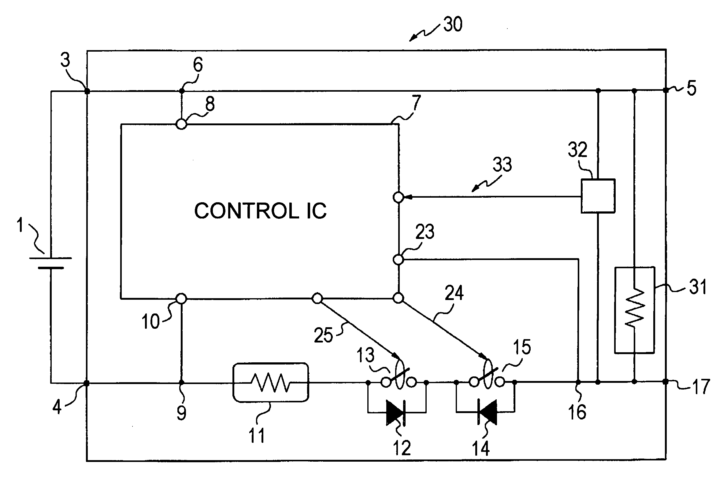
[0083]Now, the present invention will be described in detail based on specific embodiments. It is to be noted that, in a first embodiment, the same reference numerals as the abovementioned prior art are used for the corresponding elements in order to avoid duplicated detailed description. Additionally, the control IC 7 should not be limited to the one as shown in the prior art and it may be replaced by any other control IC.
[0084]FIG. 1 shows a simplified circuit schematic of the first embodiment of the battery pack protection circuit 30 according to the present invention. As for a battery cell 1 to be connected to the protection circuit 30 may be either a primary battery or a secondary battery. Moreover, the battery cell 1 may comprise a combination of more than one batteries. For example, it may be a series connection of two battery cells.
[0085]The battery cell 1 and the protection circuit 30 are accommodated in a battery pack. The protection circuit 30 is provided with a resistor ...
third embodiment
[0104]In the third embodiment, a voltage detector is used as the detector 32. In case when the voltage detector detects that the voltage between the external plus terminal 5 and the external minus terminal 17 is equal to or higher than the predetermined voltage, a discharging switch connection signal 52 from the detector 32 is applied to the processor 51.
[0105]A discharging switch connection signal 53 is also applied to the processor 51 from the control IC 7. The processor 51 calculates the discharging switch connection signal 52 and the discharging switch connection signal 53 and a calculated signal 54 recovers the ON (closed) condition, i.e., the normal condition of the discharging control switch 13, for example, when the both signals are HIGH.
[0106]As described hereinabove, since it is sufficient if the discharging control switch 13 is controlled by the signal from the detector 32, the circuit configuration is not limited to the shown embodiment. For example, it is possible to co...
fourth embodiment
[0108]In the fourth embodiment, a discharging switch connection signal 61 from the control IC 7 is applied to the discharging control switch 13 by way of a reverse current prevention device (diode) 62. A resistor 63 is connected between the gate terminal and the source terminal of the field effect transistor defining the discharging control switch 13.
[0109]Also, a voltage dropper (Zener diode) is used as the detector 32. In case when the voltage on the external plus terminal 5 exceeds the break-down voltage of the detector (Zener diode) 32, a discharging switch connection signal 64 is applied to the discharging control switch (Field Effect Transistor) 13, i.e., the gate terminal of the field effect transistor defining the discharging control switch 13. By applying the discharging switch connection signal 64 to the discharging control switch 13, the discharging control switch 13 is turned to the ON condition, or returning to the normal condition.
[0110]FIG. 6 is a simplified circuit s...
PUM
 Abstract
Description
Claims
Application Information