Mirror structure with single crystal silicon cross-member

a mirror structure and silicon cross-member technology, applied in the field of spatial light modulators, can solve the problems of virtually no memory effect and fracture, and achieve the effects of fewer micro defects and cracks, strong and reliable, and no memory

Inactive Publication Date: 2008-05-06
MIRADIA INC
View PDF70 Cites 4 Cited by
  • Summary
  • Abstract
  • Description
  • Claims
  • Application Information

AI Technical Summary

Benefits of technology

[0016]The micro mirror array includes a controllably deflectable mirror plate with a highly reflective surface to reflect incident light. The mirror plate is connected to a cross-member by a connector, both of which are substantially concealed under the reflective surface. The cross-member connects to the corners of a base that is also part of the second substrate, as there is no spacer support frame or walls between the mirrors. In an example described herein, the absence of walls surrounding the mirrors allow for larger mirror size and a higher fill ratio than designs including walls. In addition, because there are no walls, the mirror plates require less space between them, maximizing the fill ratio and contrast ratio for the array.
[0018]Further, because the cross-member is fabricated from a single crystal silicon material in one embodiment, the resulting cross-member is stronger and more reliable and suffers from virtually no memory effect, fractures along grain boundaries or fatigue. A single crystal silicon substrate has significantly fewer micro defects and cracks than other materials, especially deposited thin films. As a result, it is less likely to fracture (or to propagate micro fractures) along grain boundaries in a device.
[0020]The SLM is fabricated with few steps, which keeps the fabrication cost and complexity low. Cavities are formed in a first side of the first substrate. In parallel, hydrogen ions are implanted on a first side of the second substrate. The first side of the first substrate is bonded to the first side of the second substrate. Then, a portion of the second substrate is cleaved off using hydrogen-induced silicon layer cleavage. Through this process, only minimal alignment (˜0.5 mm) of the wafers is needed, and no thinning of the silicon wafer is required. Then a cross-member and electrodes are etched in the second substrate, a sacrificial material is deposited in the area around the cross-member, a reflective surface is deposited to create a mirror plate, the mirror plate is released by etching, to remove the sacrificial layer around the cross-member.
[0021]The net result is an easily manufacturable SLM that can achieve high optical efficiency and performance to produce high quality images reliably and cost-effectively.

Problems solved by technology

Further, because the cross-member is fabricated from a single crystal silicon material in one embodiment, the resulting cross-member is stronger and more reliable and suffers from virtually no memory effect, fractures along grain boundaries or fatigue.

Method used


Image

  • Mirror structure with single crystal silicon cross-member
  • Mirror structure with single crystal silicon cross-member
  • Mirror structure with single crystal silicon cross-member

Examples


Embodiment Construction

Spatial Light Modulator Overview

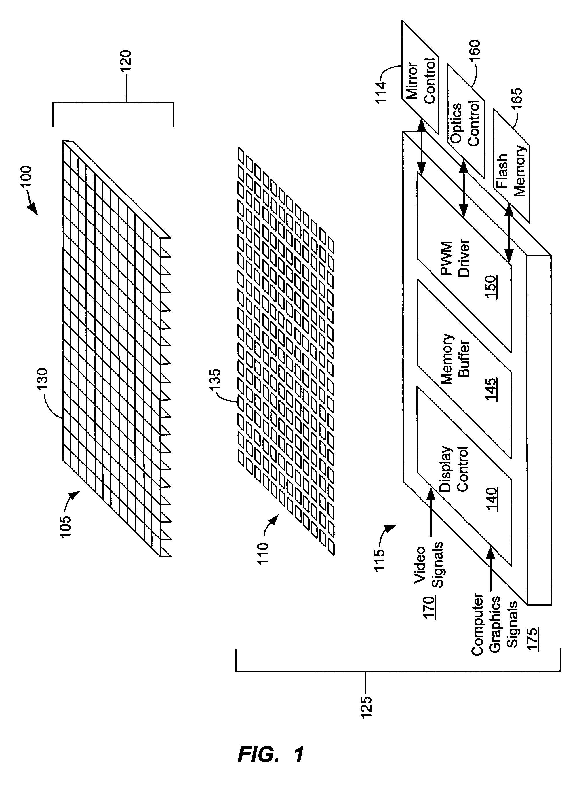
[0030]Referring now to FIG. 1, there is shown a schematic diagram that illustrates the general architecture of a SLM 100 according to one embodiment of the invention. In this example, the SLM 100 has three layers. The first layer is a mirror array 105, the second layer is an electrode array 110, and the third layer is a layer of control circuitry 115.

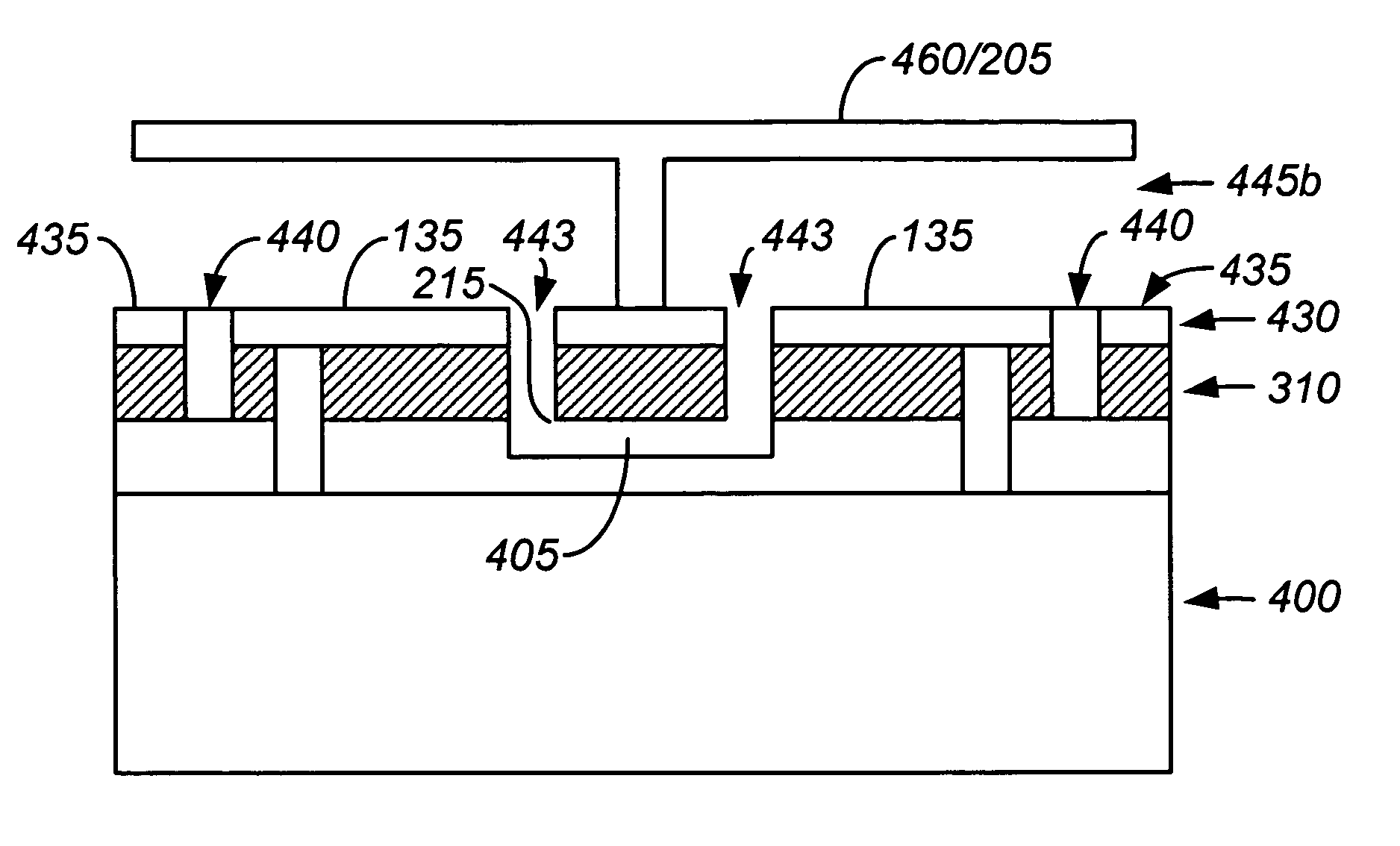
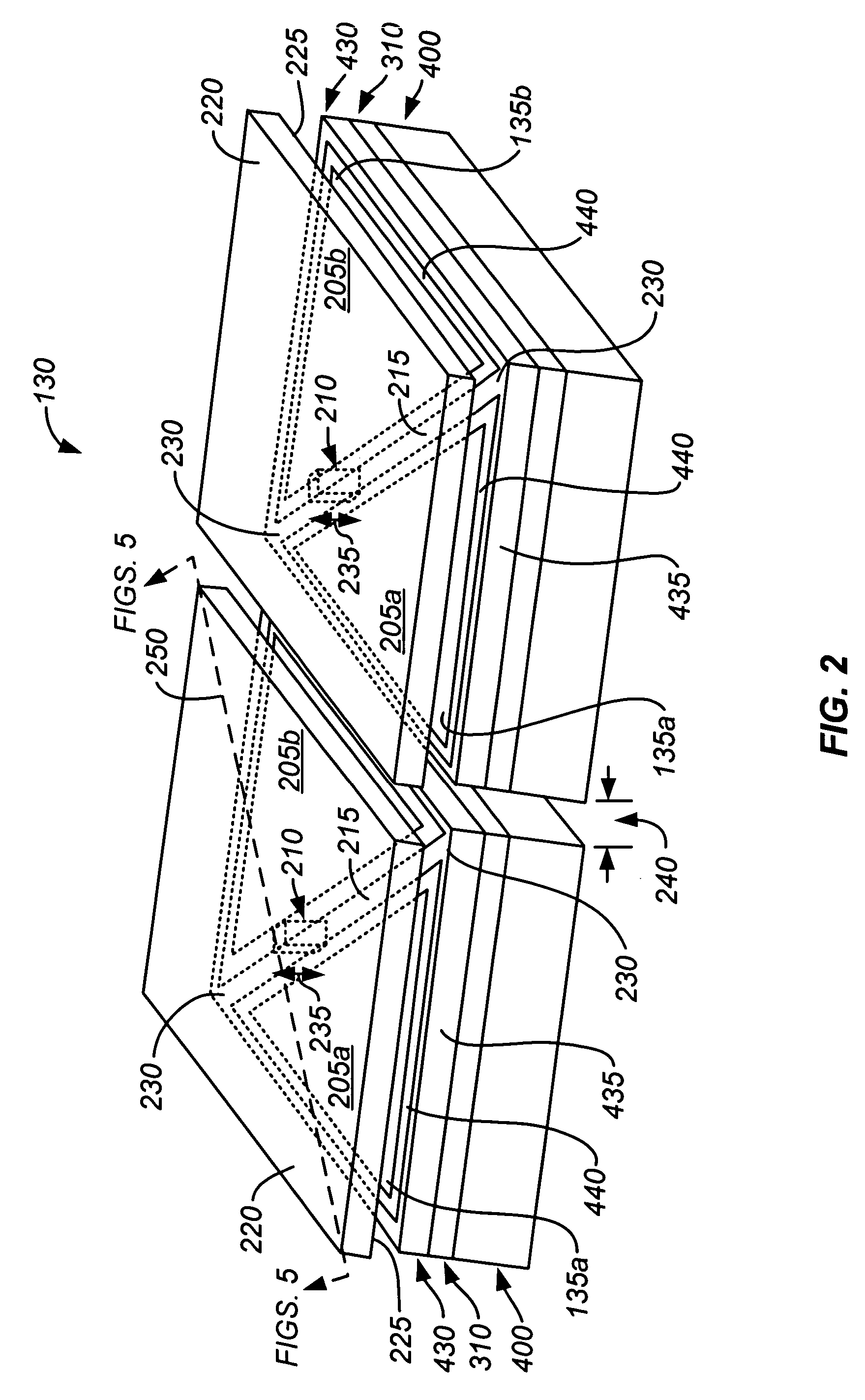
[0031]In one embodiment, the mirror array 105 is fabricated from a first substrate / layer 120 that, upon completion of fabrication, is a single material, such as single crystal silicon in the SLM 100. The mirror array 105 has a plurality of deflectable micro mirrors 130.

[0032]The electrode array 110 has a plurality of electrodes 135 for controlling the micro mirrors 130. Each electrode 135 is associated with a micro mirror 130 and controls the deflection of that micro mirror 130. Addressing circuitry allows selection of a single electrode 135 for control of the particular micro mirror 130 associated with t...


PUM

PropertyMeasurementUnit
distanceaaaaaaaaaa
temperatureaaaaaaaaaa
sizesaaaaaaaaaa

Abstract

Hydrogen cleave silicon process for light modulating mirror structure using single crystal silicon as the base cross-member. Existing processes use two critical alignment steps that can contribute to higher actuation voltages and result in lower manufacturing yields. The hydrogen cleave process simplifies the manufacturing process to one step: transferring a thin film of single crystal silicon to the CMOS substrate, resulting in minimal alignment error and providing large bonding area.

Description

CROSS-REFERENCES TO RELATED APPLICATIONS[0001]This application is a continuation of U.S. application Ser. No. 10 / 871,150, filed Jun. 18, 2004, now U.S. Pat. No. 7,042,619 entitled “Mirror Structure with Single Crystal Silicon Cross-Member,” the disclosure of which is incorporated herein by reference in its entirety.BACKGROUND OF THE INVENTION[0002]1. Field of the Invention[0003]This invention relates to spatial light modulators (SLMs), and more particularly to a micro mirror structure with hidden cross-members to maximize pixel fill ratio, minimize scattering and diffraction, and achieve a high contrast ratio and high image quality.[0004]2. Background[0005]Spatial light modulators (SLMs) have numerous applications in the areas of optical information processing, projection displays, video and graphics monitors, televisions, and electrophotographic printing. Reflective SLMs are devices that modulate incident light in a spatial pattern to reflect an image corresponding to an electrical...

Claims


Application Information

Patent Timeline
Patent Type & Authority Patents(United States)
IPC IPC(8): G02B26/00
CPCG02B26/0841
Inventor MCGINLEY, BRIAN K.MOHN, JONATHAN D.WOO, HOWARD
Owner MIRADIA INC
Why Eureka
Try Eureka