Multi-stack chip size packaging method
- Summary
- Abstract
- Description
- Claims
- Application Information
AI Technical Summary
Benefits of technology
Problems solved by technology
Method used
Image

Examples
Embodiment Construction
[0013]A preferred embodiment in accordance with the present invention will now be described with reference to the accompanying drawings.
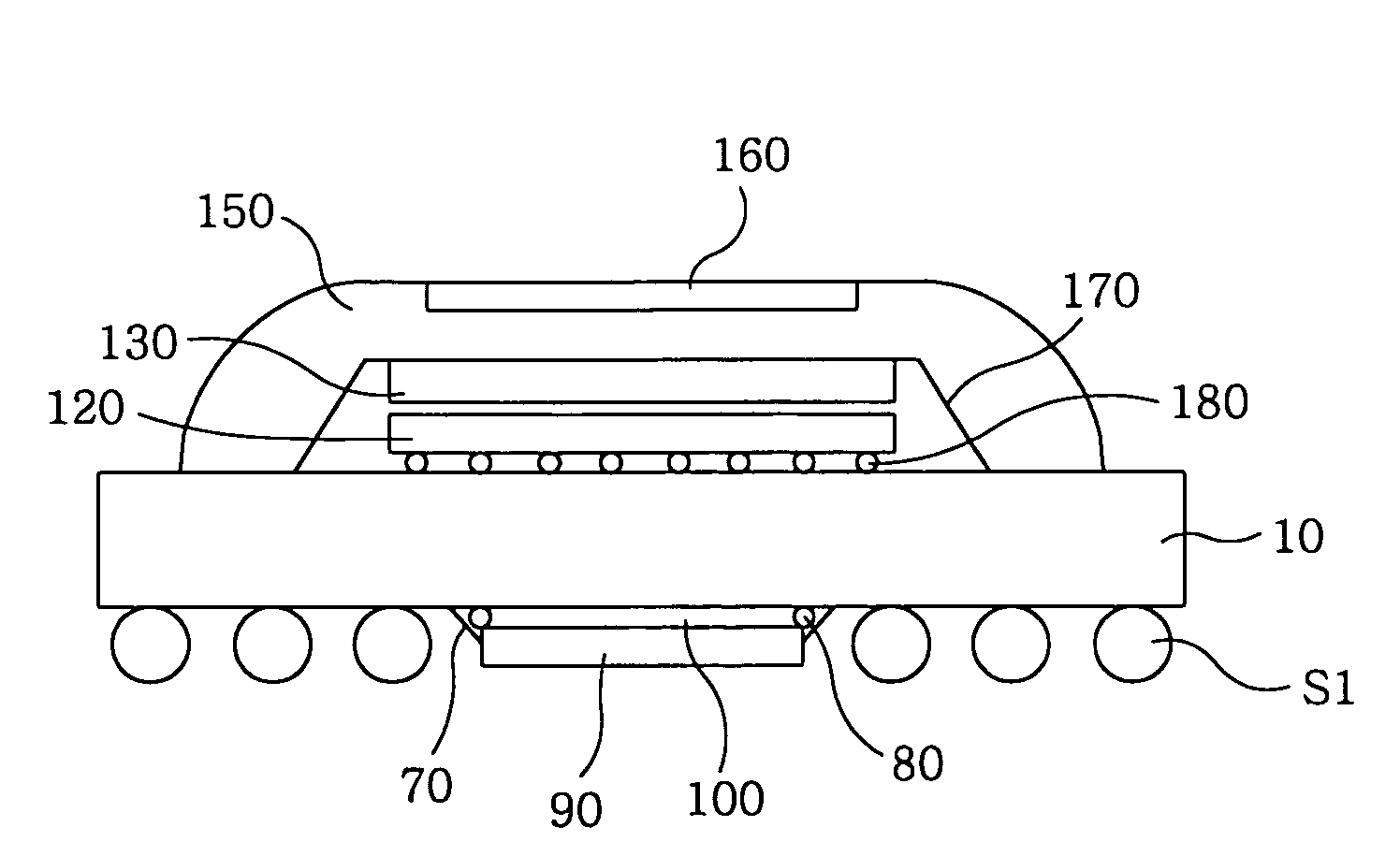
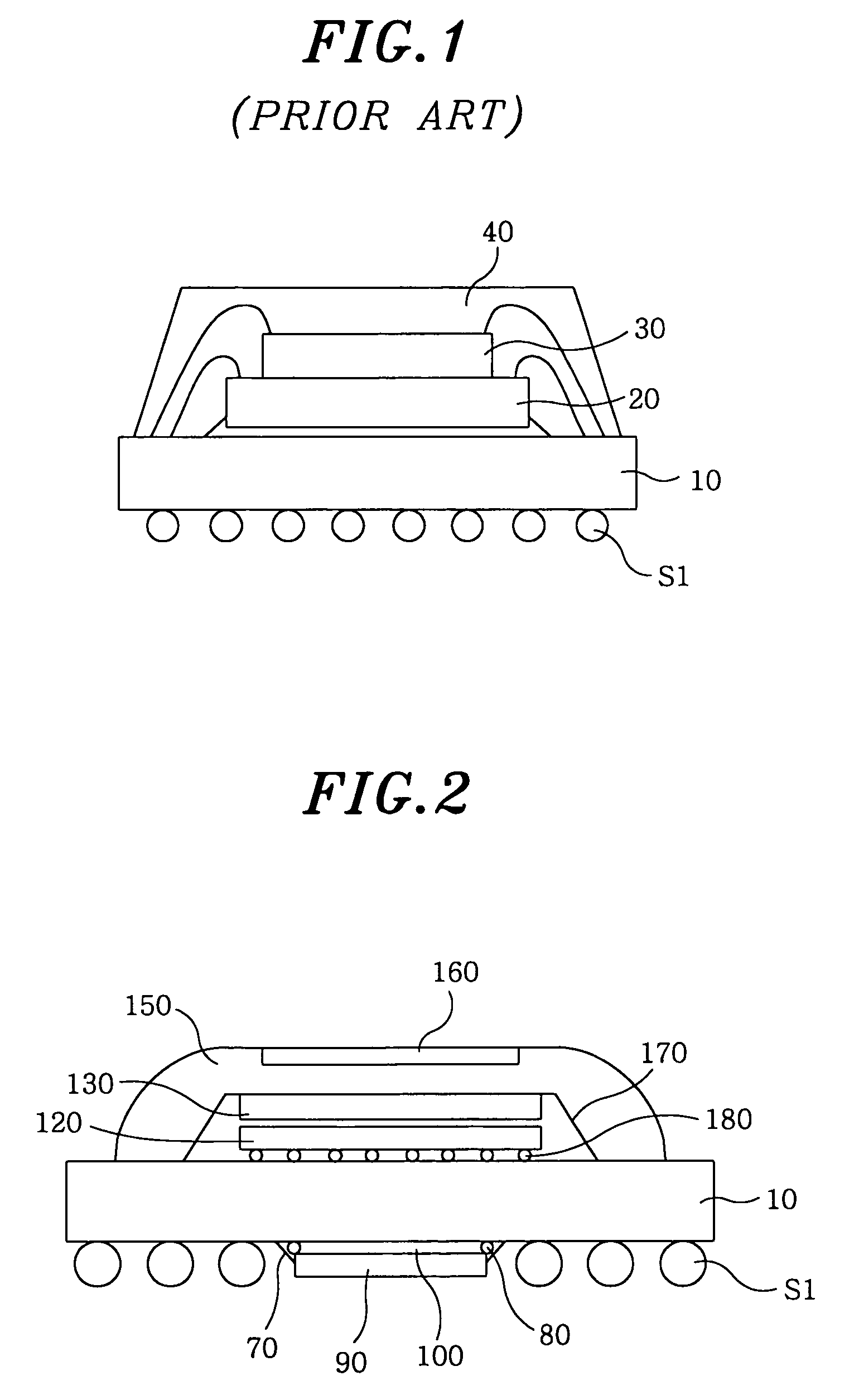
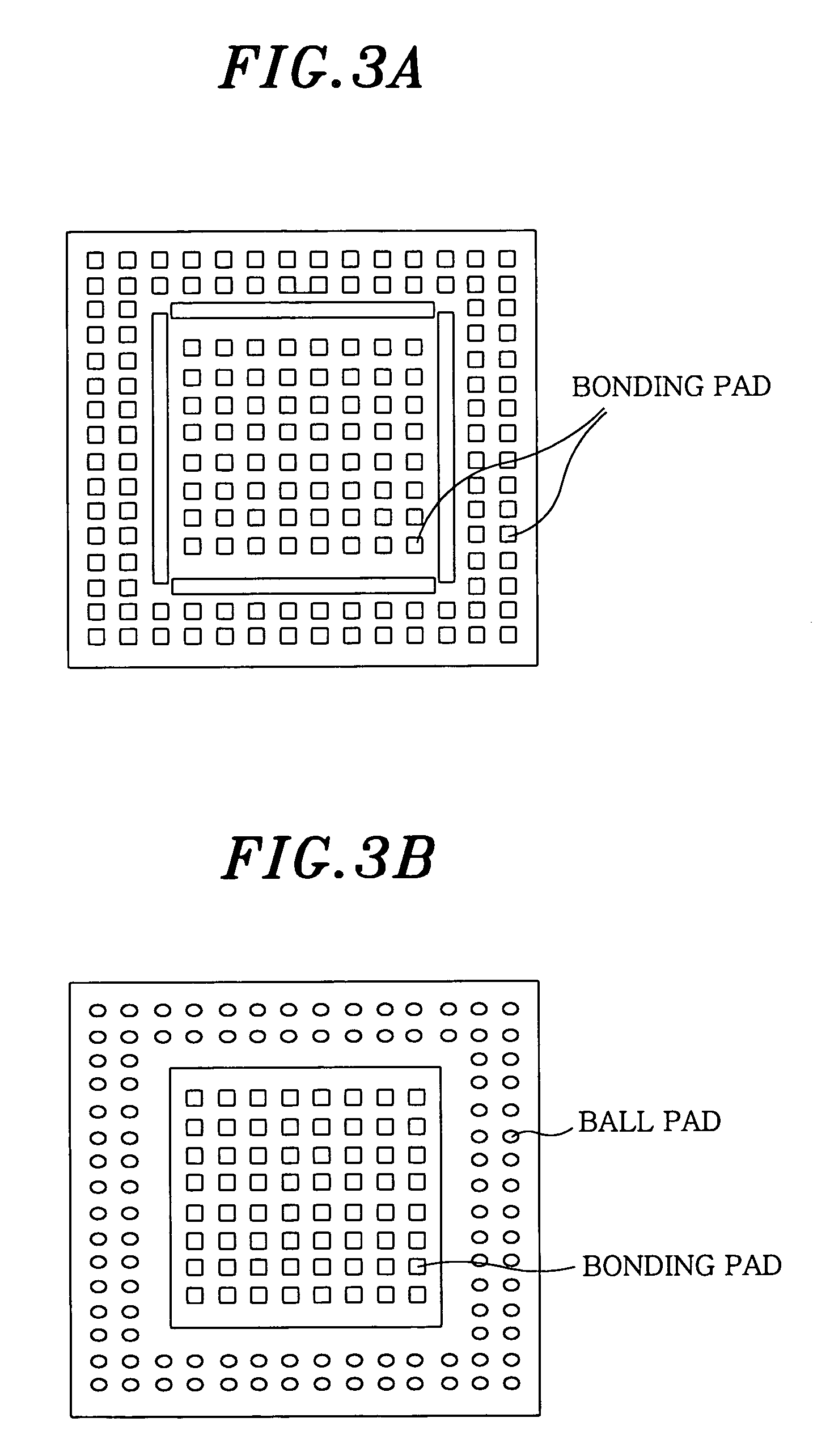
[0014]FIG. 2 illustrates a cross sectional view of a multi-stack chip size packaged (CSP) device in accordance with a preferred embodiment of the present invention. FIGS. 3A and 3B depict a top and a bottom view of the multi-stack chip sized packaged device in accordance with the preferred embodiment of the present invention.
[0015]Referring to FIGS. 2 to 3B, a first chip 120, e.g., a flip chip, is electrically interconnected to a top surface of a rigid or flexible substrate 10, e.g., a printed circuit board (PCB), through a bump 180 therebetween. Next, an epoxy is coated on the first chip 120 and a second chip 130 is stacked thereon. The second chip 130 is electrically interconnected to the PCB through an inner lead boding (ILB) scheme 170. And then, an insulating potting solution is coated on the second chip 130 and cured. A heat spreader 160 is mo...
PUM
 Abstract
Description
Claims
Application Information
 - Generate Ideas
- Intellectual Property
- Life Sciences
- Materials
- Tech Scout
- Unparalleled Data Quality
- Higher Quality Content
- 60% Fewer Hallucinations
Browse by: Latest US Patents, China's latest patents, Technical Efficacy Thesaurus, Application Domain, Technology Topic, Popular Technical Reports.
© 2025 PatSnap. All rights reserved.Legal|Privacy policy|Modern Slavery Act Transparency Statement|Sitemap|About US| Contact US: help@patsnap.com