Method and apparatus for testing function of active microstructural elements and method for producing microstructural elements using the test method

a technology of active microstructural elements and test methods, applied in individual semiconductor device testing, semiconductor/solid-state device testing/measurement, instruments, etc., can solve problems such as malfunction-free elements, malfunctions that cannot be detected, and known errors that also occur during production, so as to improve test reliability and error characterization, the effect of increasing the test tim

Inactive Publication Date: 2008-05-20
ETEC SYST INC
View PDF2 Cites 0 Cited by
  • Summary
  • Abstract
  • Description
  • Claims
  • Application Information

AI Technical Summary

Benefits of technology

[0008]Therefore, the problem addressed by the invention is to provide a method and an apparatus for testing the function of microstructural elements using particle radiation and a method for the production of microstructural elements, allowing a more precise malfunction definition.
[0012]Since the number of microstructural elements on a substrate is usually in the region of several million and the number of malfunctioning elements should be substantially less than one thousand, a test time shorter by at least a factor of one thousand results for the method according to the invention for the further test sequences. Therefore, it is readily possible to improve the test reliability and the error characterization by further test sequences without substantially increasing the test time.

Problems solved by technology

Accordingly, the known errors also occur during production, caused, for example, by contaminants or misalignments.
However, testing microstructural elements places special requirements on the method used and the corresponding apparatus owing to the small dimensions.
However, all known contract-free methods detect malfunction-free elements as malfunctioning if the error thresholds for the evaluation are set too close to the desired values of the measurement signals.
On the other hand, if a sufficient difference between the desired values and threshold values is set, malfunctions might not be detected.
Furthermore, only result data within a very restricted range are available for malfunction classifications as a result of the conventional tests.

Method used


Image

  • Method and apparatus for testing function of active microstructural elements and method for producing microstructural elements using the test method
  • Method and apparatus for testing function of active microstructural elements and method for producing microstructural elements using the test method
  • Method and apparatus for testing function of active microstructural elements and method for producing microstructural elements using the test method

Examples


Embodiment Construction

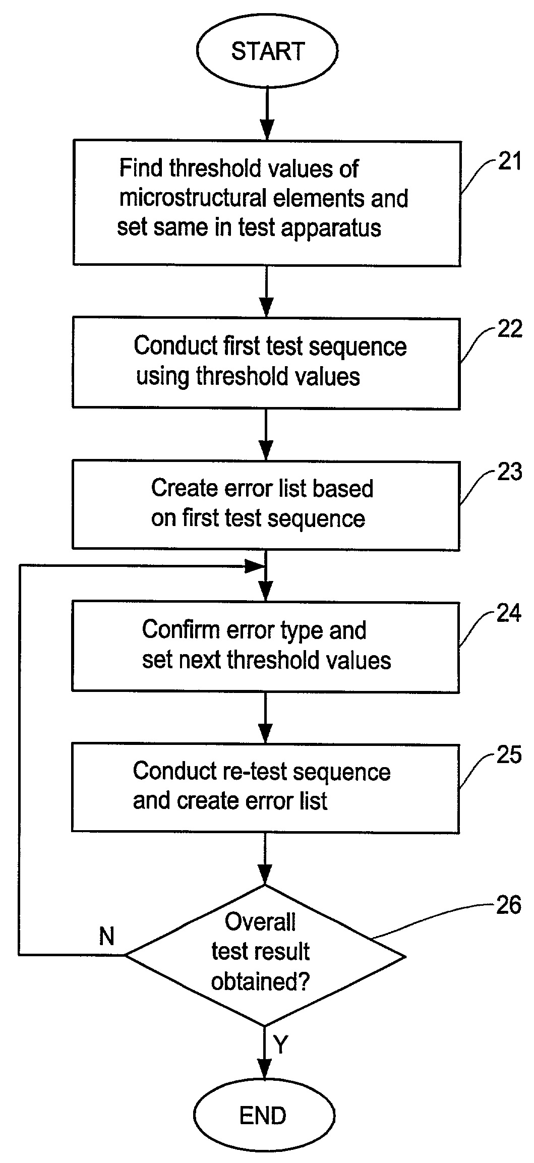
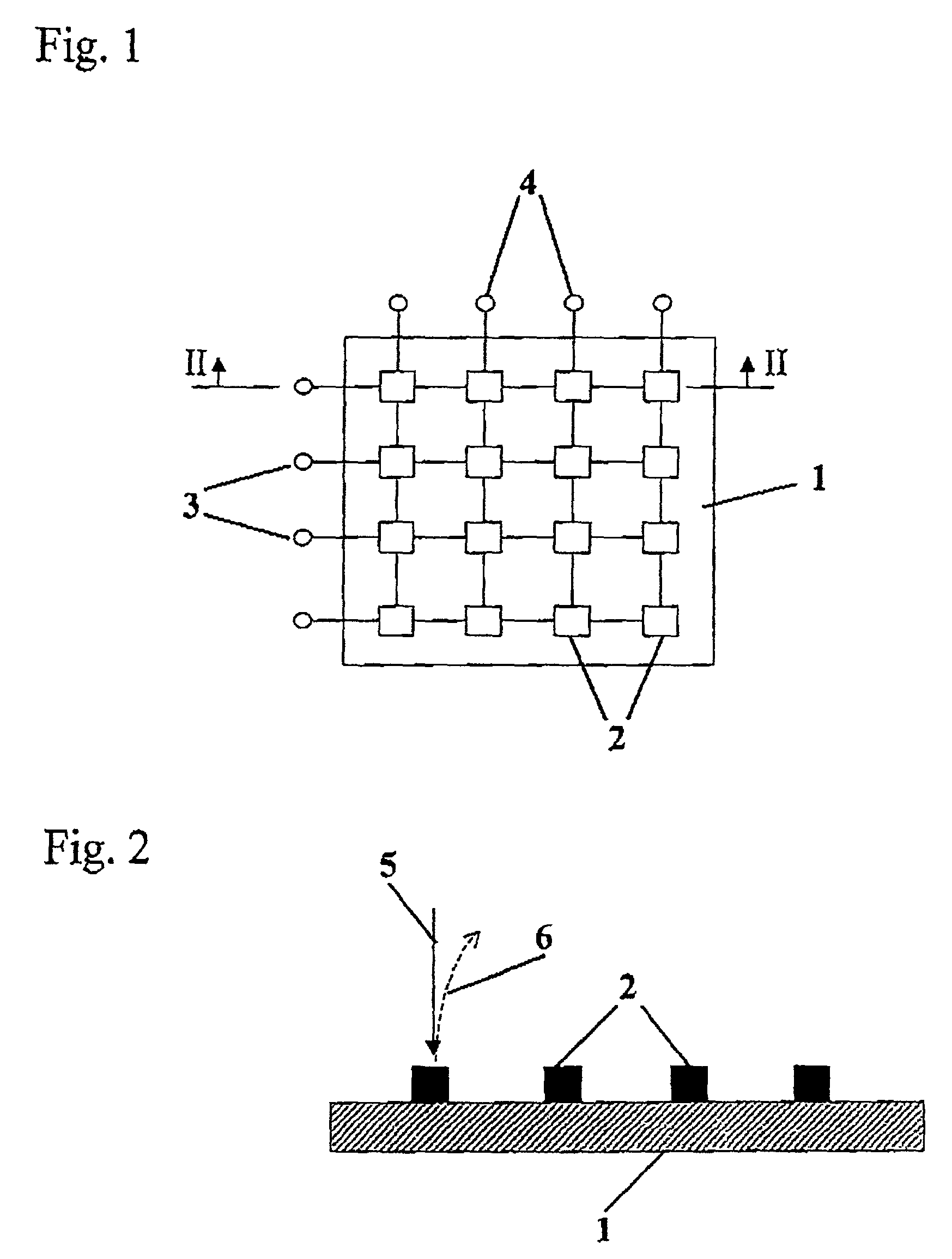
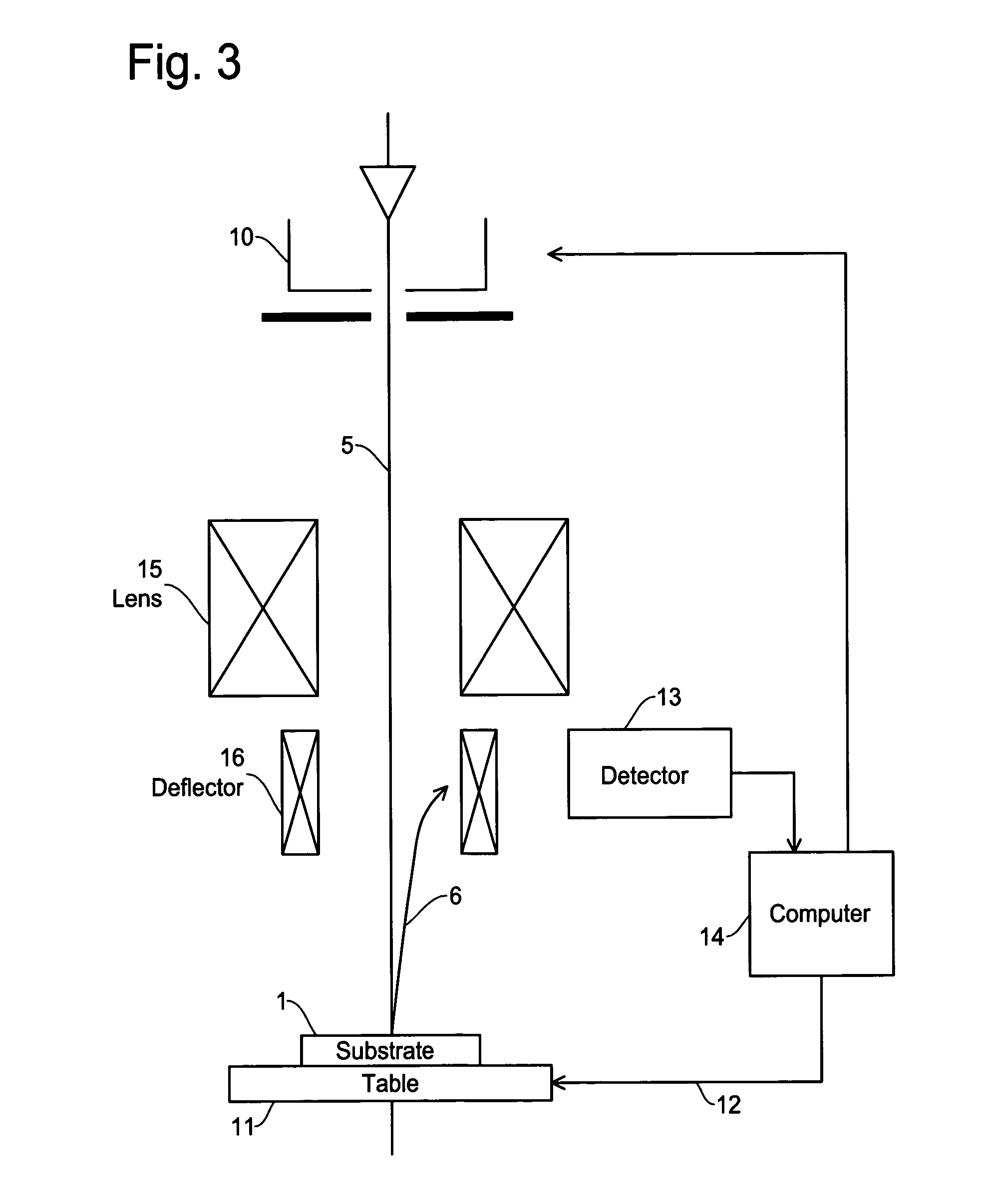
[0018]In FIGS. 1-3, a substrate 1, for example, a semiconductor wafer or liquid crystal display panel, is depicted and has a plurality of microstructural elements, the microstructural elements 2 being controllable by means of lines 3 and 4. FIG. 4 shows an operational flow of the test method of the present invention.

[0019]Possible microstructural elements include, for example, elements of the microelectronics sector (such as transistors, diodes, metal-insulator-metal elements), image elements and displays, electron structures of micromechanical sensors and actuators as well as elements (such as laser diodes or field emission tips) which emit particle radiation (for example, light or electrons). The electrical and / or mechanical properties, for example, can be tested for such microstructural elements. In addition, tests in respect of the emission properties are of interest for some microstructural elements, such as, for example, laser diodes or field emission tips.

[0020]The term elect...


PUM

PropertyMeasurementUnit
thresholdaaaaaaaaaa
voltageaaaaaaaaaa
thresholdaaaaaaaaaa

Abstract

A method and an apparatus for testing the function of a plurality of microstructural elements by irradiation with particle radiation. All of the microstructural elements detected as malfunctioning are listed in a first error list in a first test sequence. The microstructural elements listed in the first error list are tested once more in at least one further test sequence and at least the result of the test sequence last carried out is evaluated to establish the overall test result. The first test sequence is designed so that, if possible, all of the microstructural elements which are actually malfunctioning are detected. The invention further relates to a method for producing microstructural elements which are constructed as a plurality on a substrate and are tested according to the above test method.

Description

[0001]This is a continuation-in-part of U.S. patent application Ser. No. 09 / 482,756 filed Jan. 13, 2000 now abandoned.FIELD OF THE INVENTION[0002]The invention relates to a method and an apparatus for testing the function of a plurality of active microstructural elements.BACKGROUND OF THE INVENTION[0003]The term active microstructural elements is intended to refer, for example, to elements of the microelectronics sector (such as transistors, diodes, metal-insulator-metal elements), image elements and displays, electrode structures of micromechanical sensors and actuators as well as elements which emit particle radiation (for example, light or electrodes), such as laser diodes or field emission tips.[0004]Microstructural elements of that type are produced as a plurality on a substrate, for example, wafers or glass plates. In the microstructural technology sector, mechanical, optical, electrical and other elements are produced using methods and processes which have been known for some...

Claims


Application Information

Patent Timeline
Patent Type & Authority Patents(United States)
IPC IPC(8): G01R31/02G01R31/302G01N23/225G01R1/06G01R31/26G01R31/307G01R31/311G02F1/13H01L21/66
CPCG01R31/307G01R31/311
Inventor BRUNNER, MATTHIASSCHMID, RALF
Owner ETEC SYST INC
Why Eureka
Try Eureka