N-type carbon nanotube field effect transistor and method of fabricating the same

a carbon nanotube and field effect technology, applied in the field of n-type carbon nanotube field effect transistors, can solve the problems of difficult to handle potassium ions, oxygen molecule cannot be easily decomposed into oxygen atoms,

Active Publication Date: 2008-06-03
SAMSUNG ELECTRONICS CO LTD
View PDF6 Cites 7 Cited by
  • Summary
  • Abstract
  • Description
  • Claims
  • Application Information

AI Technical Summary

Problems solved by technology

However, an oxygen molecule cannot be easily decomposed into oxygen atoms and it is difficult to handle potassium ions.

Method used


Image

  • N-type carbon nanotube field effect transistor and method of fabricating the same
  • N-type carbon nanotube field effect transistor and method of fabricating the same
  • N-type carbon nanotube field effect transistor and method of fabricating the same

Examples


Embodiment Construction

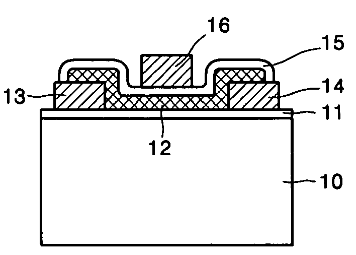
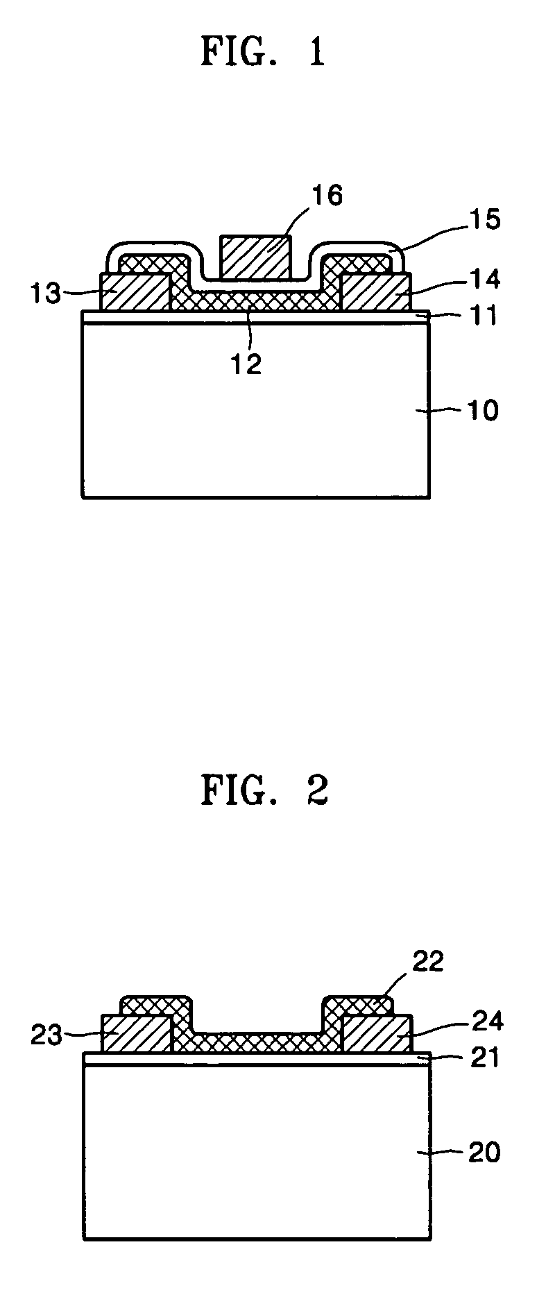
[0024]Hereinafter, an n-type carbon nanotube field effect transistor (CNT FET) having an n-type CNT and a method of fabricating the n-type CNT FET according to embodiments of the disclosure will be described in detail with reference to the attached drawings.

[0025]FIG. 1 is a cross-sectional view of an n-type CNT FET according to an embodiment of the disclosure.

[0026]Referring to FIG. 1, an insulating layer 11 may be formed on a substrate 10. A CNT 12 may be formed on the insulating layer 11 and electrodes 13 and 14 may be formed on both ends of the CNT 12, respectively. The electrodes 13 and 14 may function as a drain region and a source region, respectively, and the CNT 12 may function as a channel region.

[0027]A gate oxide layer 15 may cover the CNT 12 and a gate electrode 16 may be formed on the gate oxide layer 15, between the electrodes 13 and 14.

[0028]The gate oxide layer 15 may be formed of an oxide and may function as an electron donor layer. The gate oxide layer 15 may cont...


PUM


Abstract

Provided are an n-type carbon nanotube field effect transistor (CNT FET) and a method of fabricating the n-type CNT FET. The n-type CNT FET may include a substrate; electrodes formed on the substrate and separated from each other; a CNT forrmed on the substrate and electrically connected to the electrodes; a gate oxide layer formed on the CNT; and a gate electrode formed on the gate oxide layer, wherein the gate oxide layer contains electron donor atoms which donate electrons to the CNT such that the CNT may be n-doped by the electron donor atoms.

Description

BACKGROUND OF THE DISCLOSURE[0001]This application claims the benefit of Korean Patent Application No. 10-2004-0078544, filed on Oct. 2, 2004, in the Korean Intellectual Property Office, the disclosure of which is incorporated herein in its entirety by reference.[0002]1. Field of the Disclosure[0003]Embodiments of the present disclosure relate to a field effect transistor (FET) having n-doped carbon nanotube (CNT) and a method of fabricating the n-type CNT FET, and more particularly, to an n-type CNT FET having n-doped CNT which may be manufactured by adsorbing electron donor atoms on a CNT layer and a method of fabricating the n-type CNT FET.[0004]2. Description of the Related Art[0005]CNTs have excellent mechanical and chemical properties and may have a long length of up to one micrometer with a diameter ranging from several nanometers to several tens of nanometers. CNTs have excellent electrical conductivity and may be applied to electronic devices. Vigorous research has been con...

Claims


Application Information

Patent Timeline
Patent Type & Authority Patents(United States)
IPC IPC(8): H01L29/08H01L35/24H01L51/00
CPCB82Y10/00H01L51/002H01L51/0525H01L51/0048H01L51/0541Y10S977/938H10K71/30H10K85/221H10K10/472H10K10/464H01L21/18B82Y40/00
Inventor BAE, EUN-JUMIN, YO-SEPPARK, WAN-JUN
Owner SAMSUNG ELECTRONICS CO LTD
Why Eureka
Try Eureka