Diamond sensors, detectors, and quantum devices

a detector and detector technology, applied in the field of diamond sensors, detectors, quantum devices, can solve the problem of inevitability of defects in every region of the material

Active Publication Date: 2014-02-06
ELEMENT SIX LTD
View PDF2 Cites 69 Cited by
  • Summary
  • Abstract
  • Description
  • Claims
  • Application Information

AI Technical Summary

Benefits of technology

[0025]The third intermediate region of material disposed between the first and second regions can be fabricated by a method suitable for forming relatively high purity diamond material which has few electron donor defects relative to the first region. The third region may also comprise few quantum spin defects relative to the second region. The third intermediate region may form definitive boundary interfaces with both the first and second regions. For example, in one arrangement a layer structure comprising at least an electron donor layer (first region), a quantum spin defect acceptor layer (second region), and an intermediate spacer layer (third region) may be provided. However, it is also envisaged that the donor and acceptor regions do not need to be layers and do not need to be separated by an intermediate layer. One alternative example is to form donor and acceptor regions, for example using implantation methods, which are laterally separated rather than vertically separated into layers. Another alternative example is a vertically stacked layer structure comprising an electron donor layer and a quantum spin defect acceptor layer but no intermediate layer. In this arrangement, the donor layer may have a concentration of electron donors which is ramped downwards towards the acceptor layer. As such, there may be no separate and readily discernable intermediate layer although there will be an identifiable intermediate region having a relatively low concentration of electron donors. In effect the electron donor layer is graduated to have different regions including a region having a relatively high concentration of electron donors and a region having a relatively low concentration of electron donors adjacent the quantum spin defect region.

Problems solved by technology

As such, there will inevitable be some defects present in every region of the material, some of which may form quantum spin defects and some of which may form electron donor defects.

Method used


Image

  • Diamond sensors, detectors, and quantum devices
  • Diamond sensors, detectors, and quantum devices
  • Diamond sensors, detectors, and quantum devices

Examples


Embodiment Construction

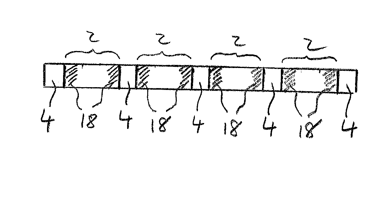
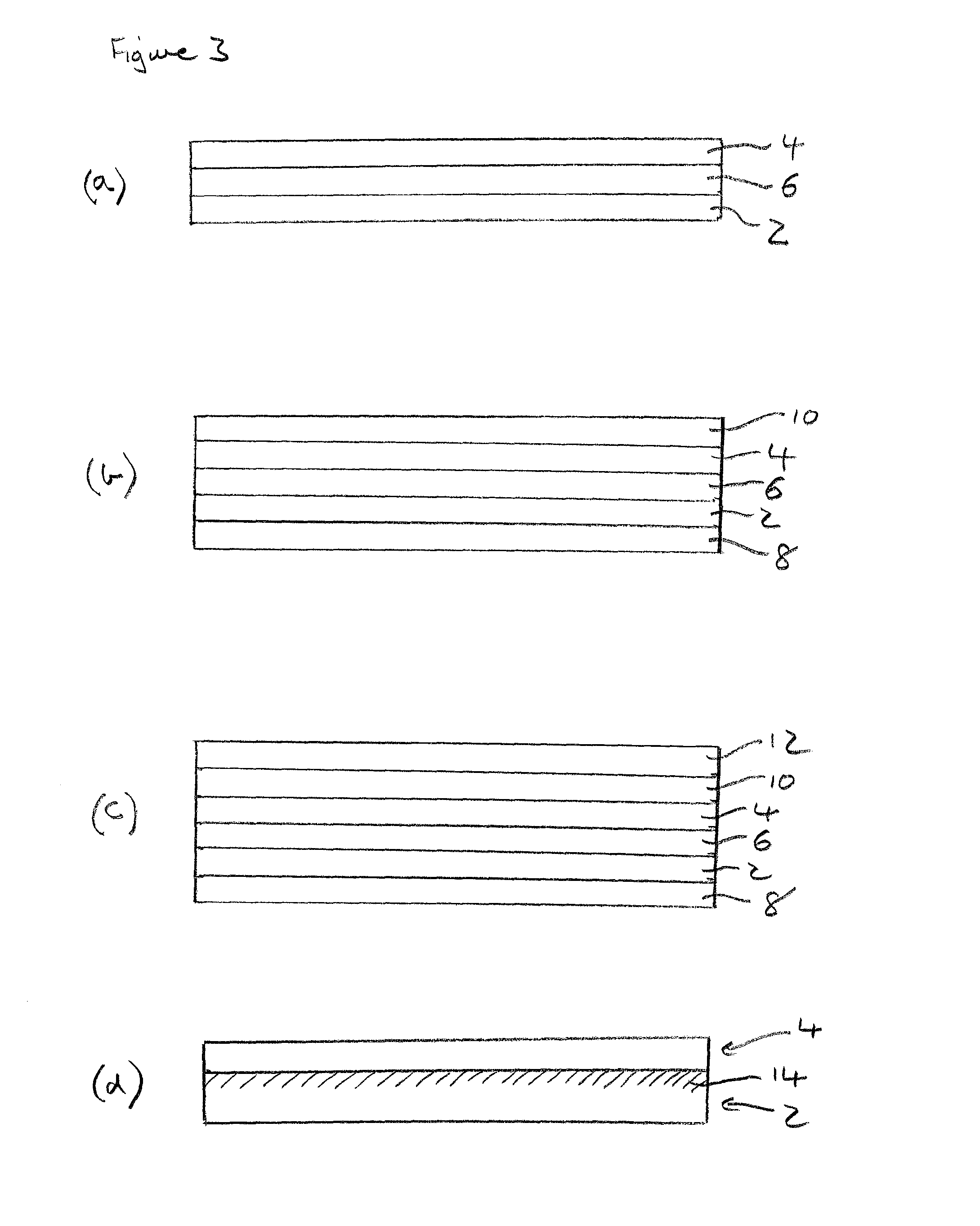
[0045]FIGS. 3(a) to 3(c) illustrate layered synthetic single crystal diamond materials according to embodiments of the present invention.

[0046]FIG. 3(a) shows a layered synthetic single crystal diamond material comprising a three layer structure. This layered structure may be entirely formed in a single crystal of synthetic diamond material such that the layers share a common crystal lattice. A first layer 2 comprises a plurality of electron donor defects. A second layer 4 comprises a plurality of quantum spin defects. A third layer 6 is disposed between the first and second layers 2, 4 such that the first and second layers 2, 4 are spaced apart by a distance in a range 10 nm to 100 μm. This distance is selected to allow electrons to be donated from the first layer 2 to the second layer 4 thus forming negatively charged quantum spin defects in the second layer 4. Furthermore, the distance between the first and second layers 2, 4 is selected to ensure dipole coupling between electron...


PUM

PropertyMeasurementUnit
thicknessaaaaaaaaaa
decoherence time T2aaaaaaaaaa

Abstract

A synthetic single crystal diamond material comprising: a first region of synthetic single crystal diamond material comprising a plurality of electron donor defects; a second region of synthetic single crystal diamond material comprising a plurality of quantum spin defects; and a third region of synthetic single crystal diamond material disposed between the first and second regions such that the first and second regions are spaced apart by the third region, wherein the second and third regions of synthetic single crystal diamond material have a lower concentration of electron donor defects than the first region of synthetic single crystal diamond material, and wherein the first and second regions are spaced apart by a distance in a range 10 nm to 100 μm which is sufficiently close to allow electrons to be donated from the first region of synthetic single crystal diamond material to the second region of synthetic single crystal diamond material thus forming negatively charged quantum spin defects in the second region of synthetic single crystal diamond material and positively charged defects in the first region of synthetic single crystal diamond material while being sufficiently far apart to reduce other coupling interactions between the first and second regions which would otherwise unduly reduce the decoherence time of the plurality of quantum spin defects and/or produce strain broaden of a spectral line width of the plurality of quantum spin defects in the second region of synthetic single crystal diamond material.

Description

FIELD OF INVENTION[0001]The present invention relates to synthetic chemical vapour deposited (CVD) diamond material for use in sensing, detecting and quantum processing applications.BACKGROUND OF INVENTION[0002]Point defects in synthetic diamond material, particularly quantum spin defects and / or optically active defects, have been proposed for use in various sensing, detecting, and quantum processing applications including: magnetometers; spin resonance devices such as nuclear magnetic resonance (NMR) and electron spin resonance (ESR) devices; spin resonance imaging devices for magnetic resonance imaging (MRI); and quantum information processing devices such as for quantum computing.[0003]Many point defects have been studied in synthetic diamond material including: silicon containing defects such as silicon-vacancy defects (Si-V), silicon di-vacancy defects (Si-V2), silicon-vacancy-hydrogen defects (Si-V:H), silicon di-vacancy hydrogen defects (S-V2:H); nickel containing defect; chr...

Claims


Application Information

Patent Timeline
Patent Type & Authority Applications(United States)
IPC IPC(8): C30B29/04
CPCC30B29/04C30B25/02C30B31/22C30B33/00G06N10/00
Inventor TWITCHEN, DANIEL JAMESMARKHAM, MATTHEW LEESCARSBROOK, GEOFFREY ALAN
Owner ELEMENT SIX LTD
Why Eureka
Try Eureka