Supercharge Your Innovation With Domain-Expert AI Agents!

Field emission display having damage prevention anode input terminal layers

a field emission display and anode input technology, applied in the field of field emission displays, can solve the problems of reducing the vacuum in the fed, unsuitable metal layer 5/b>, negatively affecting the overall operation of the display, etc., to prevent the reduction of the strength of a thin metal layer and prevent the reduction of the vacuum level

Inactive Publication Date: 2008-06-03
SAMSUNG SDI CO LTD
View PDF12 Cites 2 Cited by
  • Summary
  • Abstract
  • Description
  • Claims
  • Application Information

AI Technical Summary

Benefits of technology

[0013]In one exemplary embodiment of the present invention, there is provided a FED that prevents a reduction in strength of a thin metal layer such that the metal layer may be used as an anode electrode while its ability to be used for its original intended purpose is maintained, and such that damage to the metal layer in the vicinity of a sealant does not occur to thereby prevent a reduction in the level of the vacuum in the display.

Problems solved by technology

However, there are problems associated with metal layer 5, and in particular, with metal layer 5 made of aluminum.
This makes metal layer 5 unsuitable for use as a terminal that receives the anode voltage.
This reduces the degree of vacuum in the FED, negatively affecting the overall operation of the display.

Method used


Image

  • Field emission display having damage prevention anode input terminal layers
  • Field emission display having damage prevention anode input terminal layers
  • Field emission display having damage prevention anode input terminal layers

Examples


Embodiment Construction

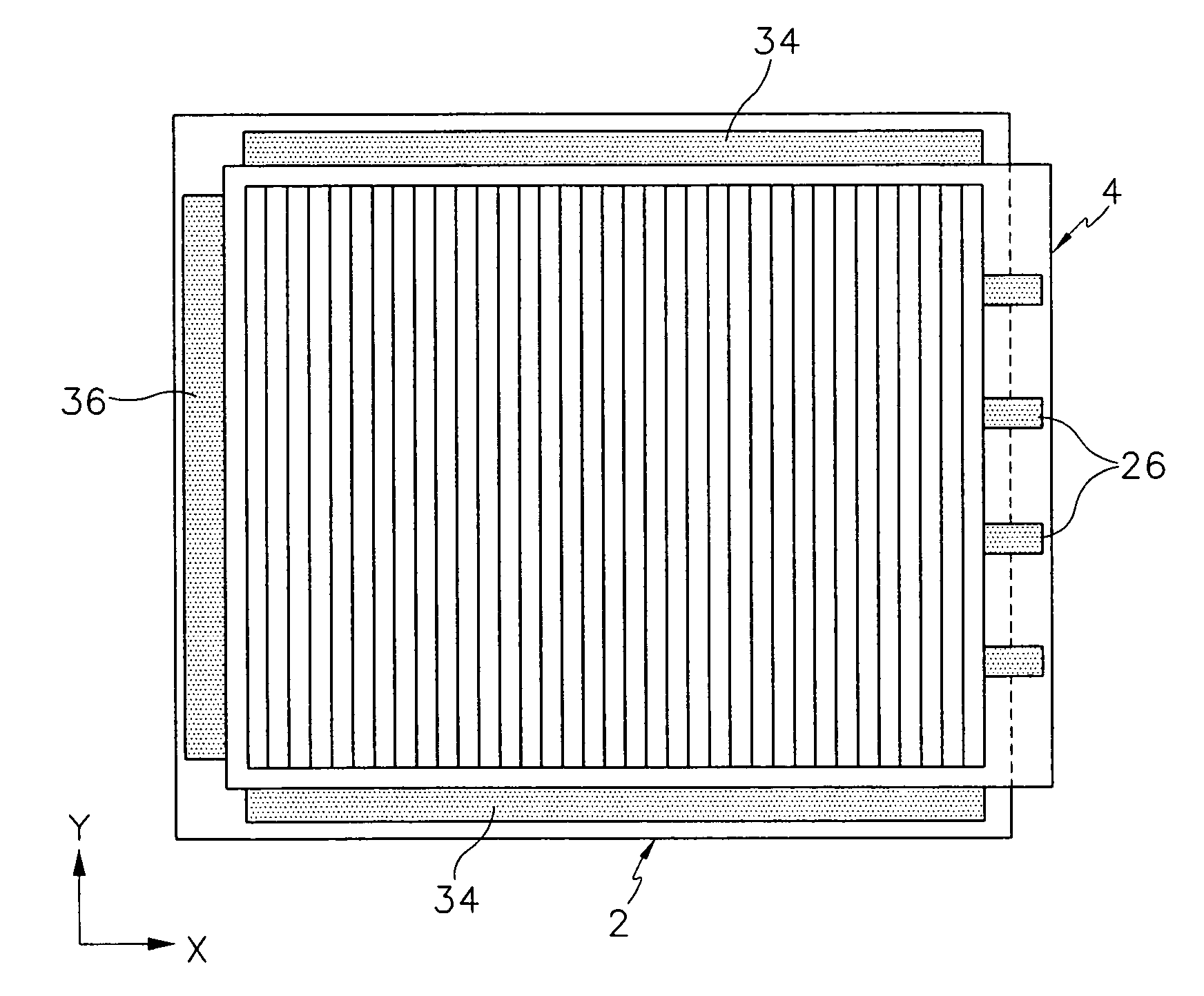
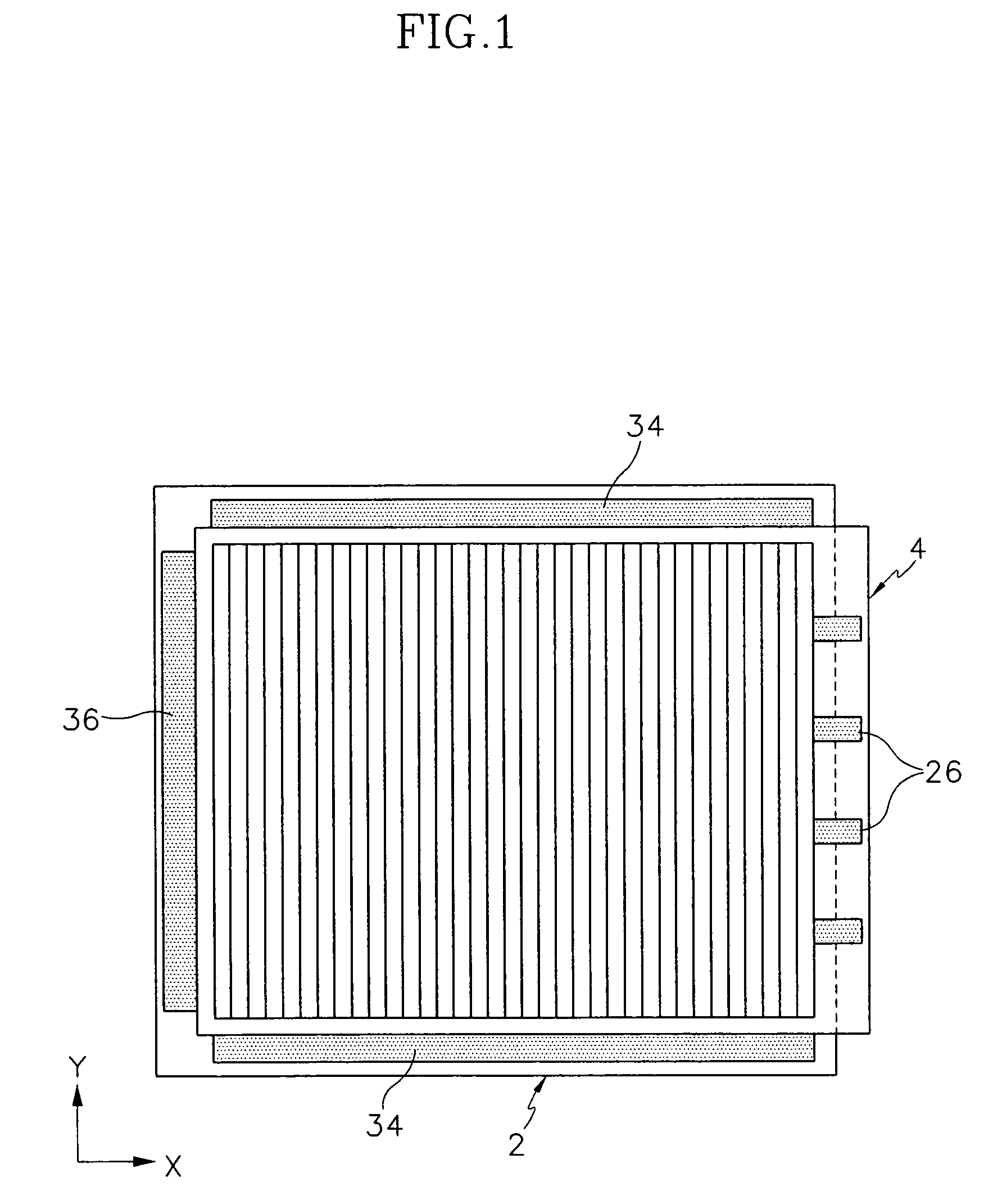
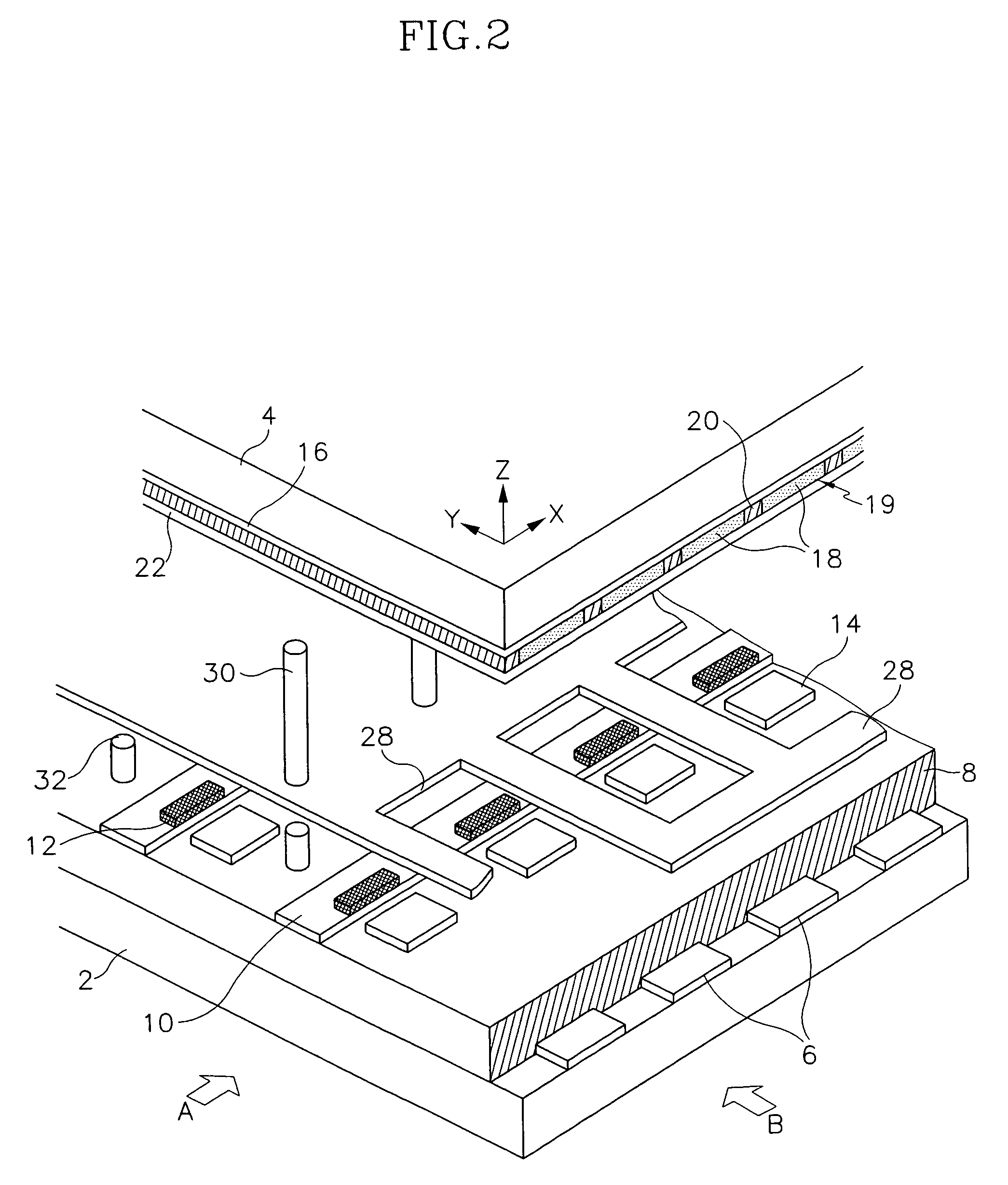
[0027]Referring to FIGS. 1-4, the FED includes backplate 2 and faceplate 4. Backplate 2 and faceplate 4 are provided opposing one another with a predetermined gap therebetween. An electron emission assembly for emitting electrons through the formation of an electric field is formed on backplate 2. An illumination assembly for realizing predetermined images by interaction with electrons is formed on faceplate 4.

[0028]In more detail, with respect to the electron emission assembly, gate electrodes 6 are formed on a surface of backplate 2 opposing faceplate 4. Gate electrodes 6 are formed in a stripe pattern and along one direction of backplate 2 (for example, direction Y). Further, insulation layer 8 is formed over an entire surface of backplate 2 covering gate electrodes 6, and cathode electrodes 10 are formed on insulation layer 8. Cathode electrodes 10 are formed in a stripe pattern and in a direction substantially perpendicular to the direction of gate electrodes 6, that is, cathod...


PUM


Abstract

A field emission display (FED). A vacuum assembly is formed with first and second substrates and a sealant. An electron emission assembly is formed on the first substrate and emits electrons by the formation of electric fields. An illumination assembly is formed on the second substrate and realizes a display of images by electrons emitted from the electron emission assembly. The illumination assembly includes a transparent conductive layer formed on the second substrate and having an anode input terminal that extends outside the vacuum assembly and to which an anode voltage is applied, a phosphor screen formed on the transparent conductive layer, and a metal layer formed on the phosphor screen within the vacuum assembly in such a manner that a portion of the metal layer contacts the transparent conductive layer.

Description

CROSS-REFERENCE TO RELATED APPLICATIONS[0001]This application claims priority to and the benefit of Korean Patent Application No. 2003-0028604 filed on May 6, 2003 in the Korean Intellectual Property Office, the entire content of which is incorporated herein by reference.BACKGROUND OF THE INVENTION[0002](a) Field of the Invention[0003]The present invention relates to a field emission display, and more particularly, to a field emission display that includes a thin metal layer formed on a phosphor screen, which is provided on a faceplate, to improve brightness and contrast.[0004](b) Description of the Related Art[0005]In a conventional field emission display (FED), there are formed on a backplate emitters that are electron emission sources, and electrodes (i.e., cathode electrodes and gate electrodes) that operate such that electrons are emitted from the emitters. A phosphor screen is formed on a surface of a faceplate opposing the backplate.[0006]With this configuration, a difference...

Claims


Application Information

Patent Timeline
IPC IPC(8): H01J63/04H01J1/62H01J1/30H01J29/08H01J31/12
CPCB82Y10/00H01J29/085H01J31/127H01J2201/30469C01B32/05H01J1/30
Inventor OH, TAE-SIK
Owner SAMSUNG SDI CO LTD
Features
  • R&D
  • Intellectual Property
  • Life Sciences
  • Materials
  • Tech Scout
  • Unparalleled Data Quality
  • Higher Quality Content
  • 60% Fewer Hallucinations
Learn More