Reconfigurable network on a chip

a reconfigurable network and chip technology, applied in the field of network processing, can solve the problems of minimizing the overall system cost, unable to meet the existing space system architecture and associated design approaches are not meeting the new design and cost requirements, etc., to facilitate the processing of large data structures, easy to program, and highly flexible

a reconfigurable network and chip technology, applied in the field of network processing, can solve the problems of minimizing the overall system cost, unable to meet the existing space system architecture and associated design approaches are not meeting the new design and cost requirements, etc., to facilitate the processing of large data structures, easy to program, and highly flexible

US7382154B2Active Publication Date: 2008-06-03HONEYWELL INT INC

Image

  • Reconfigurable network on a chip
  • Reconfigurable network on a chip
  • Reconfigurable network on a chip

Examples


Embodiment Construction

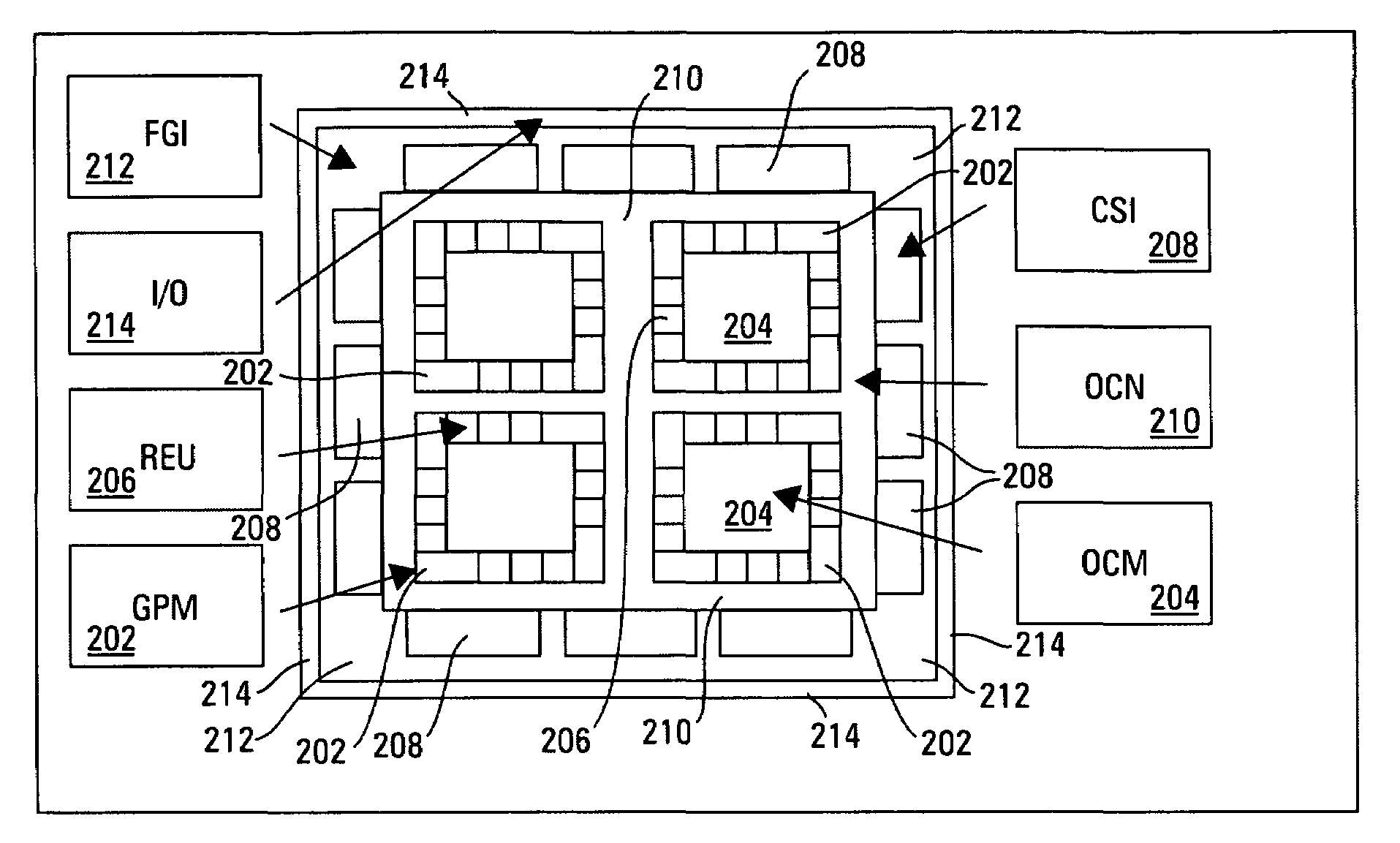
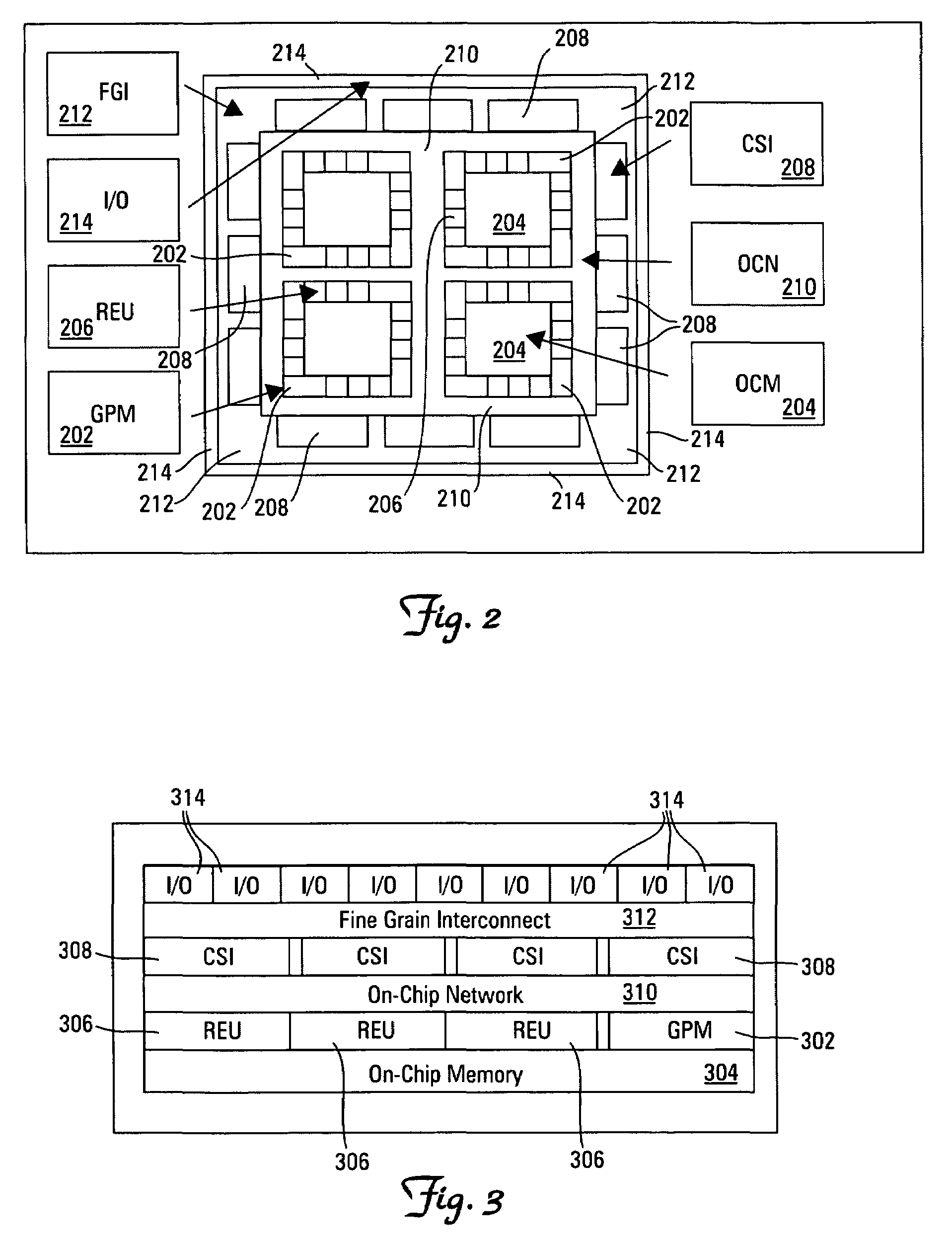
[0017]With reference again to the figures, FIG. 2 depicts a block diagram of an example architecture for a reconfigurable network 200, which can be used to implement a preferred embodiment of the present invention. As shown, for this example embodiment, reconfigurable network 200 in FIG. 2 is arranged in a particular configuration as a plurality of network processing resources on a semiconductor chip. However, it should be understood that the present invention is not intended to be so limited and can also include within its scope any suitable arrangement and / or number of the network processing resources shown. The actual number and arrangement of the network processing resources is dictated to a great extent by the technology of the target semiconductor processes or applications involved. Also, the present invention is not intended to be limited only to a semiconductor chip. As such, for this example embodiment, reconfigurable network 200 includes sixteen general purpose microproces...


PUM


Abstract

An architecture for a reconfigurable network that can be implemented on a semiconductor chip is disclosed, which includes a hierarchical organization of network components and functions that are readily programmable and highly flexible. Essentially, a reconfigurable network on a chip is disclosed, which includes aspects of reconfigurable computing, system on a chip, and network on a chip designs. More precisely, a reconfigurable network on a chip includes a general purpose microprocessor for implementing software tasks, a plurality of on-chip memories for facilitating the processing of large data structures as well as processor collaboration, a plurality of reconfigurable execution units including self-contained, individually reconfigurable programmable logic arrays, a plurality of configurable system interface units that provide interconnections between on-chip memories, networks or buses, an on-chip network including a network interconnection interface that enables communication between all reconfigurable execution units, configurable system interface units and general purpose microprocessors, a fine grain interconnect unit that gathers associated input / output signals for a particular interface and attaches them to a designated system interface resource, and a plurality of input / output blocks that supply the link between an on-chip interface resource and a particular external network or device interface. Advantageously, the network minimizes the configuration latency of the reconfigurable execution units and also enables reconfiguration on-the-fly.

Description

FIELD OF THE INVENTION[0001]The present invention relates generally to the network processing field, and more specifically, but not exclusively, to an architecture for a reconfigurable network that can be implemented on a semiconductor chip.BACKGROUND OF THE INVENTION[0002]The desire by mission planners to implement viable space communication infrastructures that can facilitate the deployment of next-generation space-based networks creates numerous design challenges for today's spacecraft system engineers. These design challenges are compounded by increasingly demanding space applications and increased mission requirements, and also significant pressure to minimize the overall system costs. Generally, the trend is to implement less costly space communication systems while striving to transport more data to and from user applications. In this regard, a major problem encountered by system designers is that the existing space system architectures and associated design approaches fall s...

Claims


Application Information

Patent Timeline
03 Jun 2008
Publication
US7382154B2
IPC
H03K19/173
CPC
G06F15/7867
Inventors
RAMOS, JEREMY; STACKELHOUSE, SCOTT D.